Optical scanner apparatus with pinhole imaging device

Inactive Publication Date: 2007-08-28
INTELLECTUAL VENTURES I LLC
View PDF1 Cites 4 Cited by
  • Summary
  • Abstract
  • Description
  • Claims
  • Application Information

AI Technical Summary

Benefits of technology

[0013]It is a further object of this invention to provide an imaging device to improve the light dispersion effect.
[0014]It is yet an object of this invention to increase the exposure to enhance the ratio of s / n (signal / noise).
[0015]According to the abovementioned objects, the present invention provides an imaging device to replace the conventional lens-imaging device in an optical scanning module of an optical scanner apparatus. The imaging device such as a pinhole-imaging device is used to replace the conventional lens-imaging device in an optical scanning module to receive the illuminant, which is transmitted from the scanning object to the pinhole-imaging device and into the optical sensor such as a CCD (charge coupled device) to form an optical image focused on the CCD. The size of the aperture of the pinhole-imaging device can be equal to or smaller than the pixel of the CCD such that the illuminant only illuminates through the apertures of the pinhole-imaging device to the CCD to reduce the light dispersion effect. Furthermore, in order to reduce the s / n (signal / noise) ratio, the scanning exposure is increased to obtain better image qualities.

Problems solved by technology

Furthermore, due to the light dispersion effect, the imaging data cannot focus completely on a point such that the resolution of the imaging data on the two ends 202A and 202B is bad.
However, the cost of the CCD 106 is proportional to the square of the number of pixels.
Furthermore, the lens-imaging device exhibits a plane to scan the scanning object 100, and the MTF (modulation transfer function) is poor when the optical sensor 106 is diverged from the plane of the lens-imaging device 104.

Method used


Image

  • Optical scanner apparatus with pinhole imaging device
  • Optical scanner apparatus with pinhole imaging device
  • Optical scanner apparatus with pinhole imaging device

Examples


Embodiment Construction

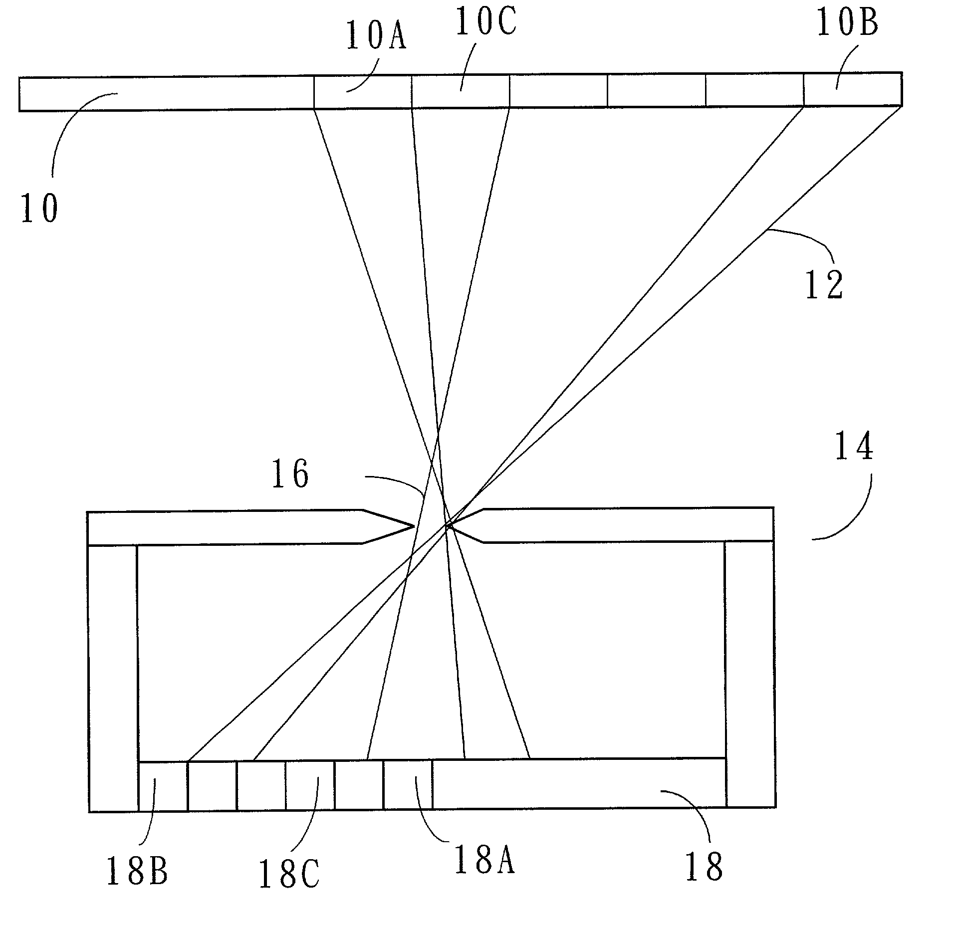
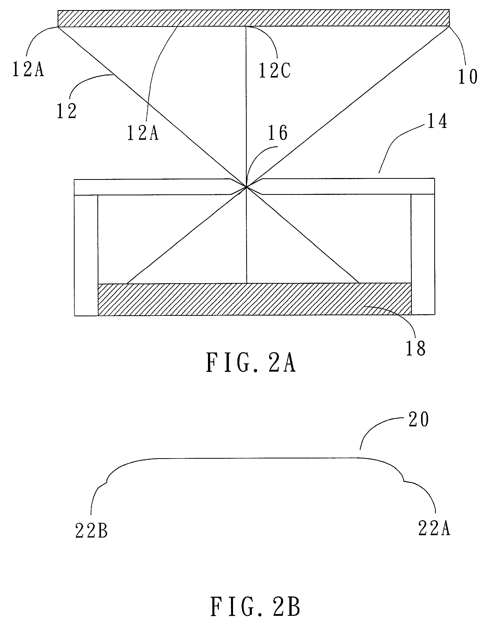
[0023]Some sample embodiments of the invention will now be described in greater detail. Nevertheless, it should be recognized that the present invention can be practiced in a wide range of other embodiments besides those explicitly described, and the scope of the present invention is expressly not limited except as specified in the accompanying claims.

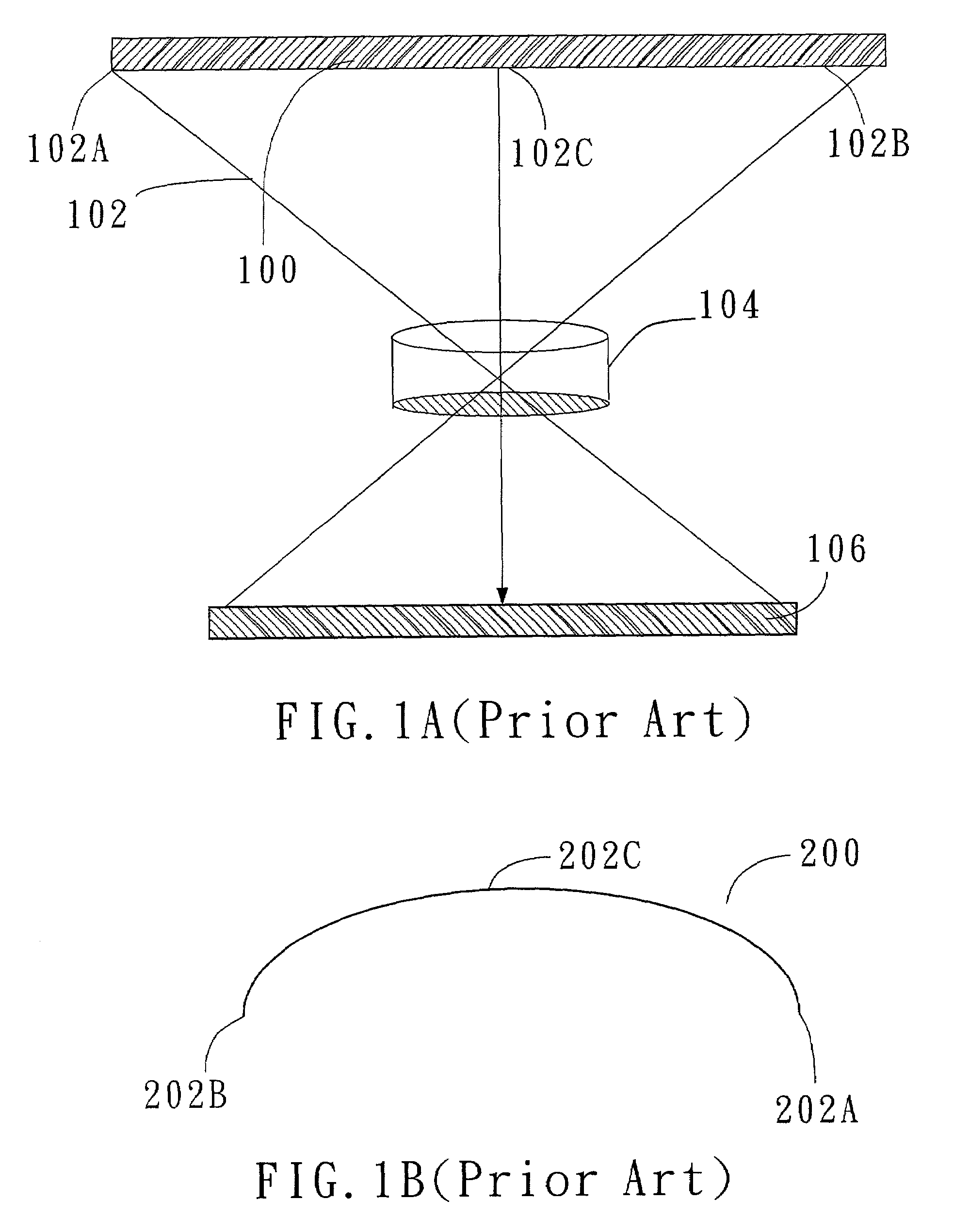
[0024]A conventional optical scanner apparatus with a lens-imaging device scans a scanning object to form an optical image which is focused on the optical sensor. The conventional optical scanner apparatus with lens-imaging device for scanning object, due to the light dispersion effect such that the imaged light cannot focus completely on the optical sensor, may cause poor resolution when the imaged light is transmitted through the lens-imaging device to the optical sensor. Therefore, the present invention provides a pinhole-imaging device used to replace the conventional lens-imaging device to improve the resolution of the optical ima...


PUM


Abstract

A pinhole-imaging device is used as an imaging device for an optical scanner apparatus. The pinhole-imaging device replaces the conventional lens-imaging device and is placed in front of the optical sensor to receive the imaged light from the scanning object and the optical image is focused on the optical sensor. When the radius of the aperture of pinhole-imaging device is smaller or equal to the pixel of the optical sensor, the imaged light transmitted through the aperture of the pinhole-imaging device is focused on the optical sensor to form an image such that the resolution of the optical imaging can be obtained and the light dispersion effect issue can be improved.

Description

BACKGROUND OF THE INVENTION[0001]1. Field of the Invention[0002]The present invention generally relates to an optical scanner apparatus, and more particularly to an imaging device of an optical scanning module to prevent the light dispersion effect and obtain the better mtf (modulation transfer function).[0003]2. Description of the Prior Art[0004]Scanner devices, such as flatbed scanners, are well known in the art and produce machine-readable image data signals that are representative of scanned object, such as a photograph or a page of printed text. In a typical scanner application, the image data signals produced by a scanner may be used by personal computer to reproduce an image of the scanned object in a suitable display device, such as a CRT (cathode ray tube) or a print.[0005]Flatbed scanners are widely used with computer systems for converting printed data into image signals. An optical scanning module is the most important component of the flatbed scanner. The scanning modul...

Claims


Application Information

Patent Timeline
IPC IPC(8): H04N1/04G01D5/34H04N1/03H04N1/10H04N1/193
CPCG01D5/34H04N1/03H04N1/1017H04N1/193H04N2201/02493
Inventor KUO, SHIH-ZHENG
Owner INTELLECTUAL VENTURES I LLC
Why Eureka
Try Eureka