
Fastplace method for integrated circuit design

a fastplace and integrated circuit technology, applied in computer aided design, program control, instruments, etc., can solve the problems of increasing the size of the day, the inability of quadratic objective alone to give the best possible wire length, and the problem of remaining, etc., to achieve efficient analytical placement, eliminate cell, and fast

Inactive Publication Date: 2007-09-04
IOWA STATE UNIV RES FOUND
View PDF1 Cites 46 Cited by
  • Summary
  • Abstract
  • Description
  • Claims
  • Application Information

AI Technical Summary

Benefits of technology

[0006]Therefore, it is a primary object, feature, or advantage of the present invention to improve over the state of the art.
[0007]It is a further object, feature, or advantage of the present invention to provide a fast, iterative, flat placement method for large-scale standard cell designs.
[0008]It is a still further object, feature, or advantage of the present invention to provide a method for efficient analytical placement for standard cell designs that eliminates cell overlap.
[0009]Another object, feature, or advantage of the present invention is to provide a method for efficient analytical placement for standard cell designs that reduces wirelength.
[0010]Yet another object, feature, or advantage of the present invention is to provide a method for efficient analytical placement for standard cell designs that speeds up the process of solving where a quadratic approach is used.
[0011]One or more of these and / or other objects, features, or advantages of the present invention will become apparent from the specification and claims that follow.

Problems solved by technology

Placement happens to be one of the most persistent challenges in present day Integrated Circuit design.
Designs in current deep sub-micron technology often contain over a million placeable components, and are getting larger by the day.
Moreover, because of the dominance of interconnect delay, placement has become a major contributor to timing closure results.
Also, the quadratic objective by itself does not give the best possible wire length.
Thus, despite various attempts and approaches at providing efficient analytical placement of cells in integrated circuit design, problems remain.

Method used


Image

  • Fastplace method for integrated circuit design
  • Fastplace method for integrated circuit design
  • Fastplace method for integrated circuit design

Examples


Embodiment Construction

1. Overview

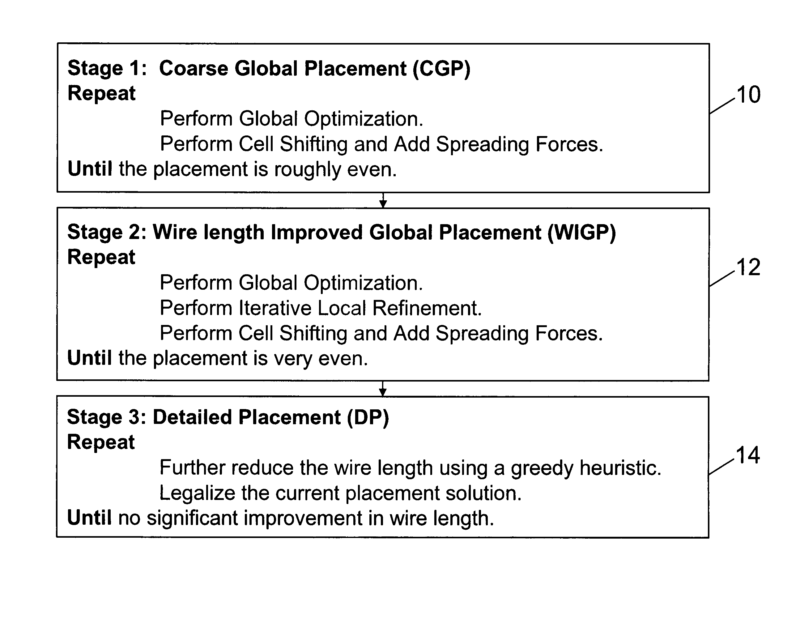
[0021]The methodology of one embodiment of the present invention is sometimes referred to as FastPlace and essentially consists of three stages as shown in FIG. 1. FIG. 1 illustrates the first stage 10, the second stage 12, and the third stage 14. The aim of the first stage is to minimize the wire length and spread the cells over the placement region to obtain a coarse global placement. It is composed of an iterative procedure in which we alternate between Global Optimization and Cell Shifting. Global Optimization involves minimizing the quadratic objective function. During Cell Shifting, the entire placement region is divided into equal sized bins and the utilization of each bin is determined. The standard cells are then shifted around the placement region based on the bin in which they lie and its current utilization. Finally, a spreading force is added to all the cells to account for their movement during shifting.

[0022]The second stage is to refine the global placemen...


PUM


Abstract

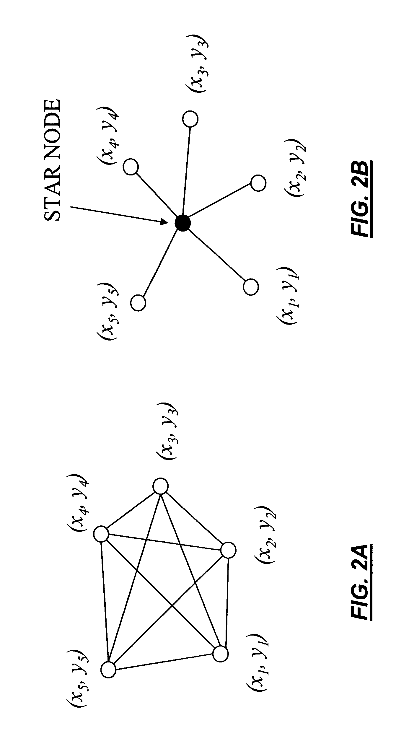
A method for efficient analytical placement of standard cell designs includes obtaining a placement of cells using a wirelength objective function, modifying the placement of cells by cell shifting to redistribute cells to thereby reduce cell overlap, and refining the placement of cells to thereby reduce wirelength using a half-perimeter bounding rectangle-measure. Preferably the wirelength the wirelength objective function is a quadratic objective function which is solved using a hybrid net model. The hybrid net model preferably uses a clique model for two-pin and three-pin nets and a star model for nets having at least four pins. The use of the hybrid net model reduces a number of non-zero entries in a connectivity matrix.

Description

BACKGROUND OF THE INVENTION[0001]The present invention relates to the field of integrated circuit design. More particularly, the present invention relates to a placement algorithm such as may be used for large-scale standard cell designs.[0002]Placement happens to be one of the most persistent challenges in present day Integrated Circuit design. Designs in current deep sub-micron technology often contain over a million placeable components, and are getting larger by the day. Moreover, because of the dominance of interconnect delay, placement has become a major contributor to timing closure results. Placement needs to be performed early in the design flow. Hence, it becomes imperative to have an ultra-fast placement tool to handle the ever increasing placement problem size.[0003]In recent years, many placement algorithms have been proposed to handle the widely-used objective of wire length minimization. These algorithms apply various approaches including analytical placement, simulat...

Claims


Application Information

Patent Timeline
Patent Type & Authority Patents(United States)
IPC IPC(8): G06F17/50
CPCG06F17/5072G06F30/392
Inventor CHU, CHRIS CHONG-NUENVISWANATHAN, NATARAJAN
Owner IOWA STATE UNIV RES FOUND
Learn More