Light source device for scanning-exposure and method and apparatus for scanning-exposure

a light source device and scanning exposure technology, applied in semiconductor lasers, inking devices, instruments, etc., can solve the problems of destroying the quality of recorded images, prior arts cannot efficiently eliminate laser flares, etc., to achieve efficient elimination of extraneous light, maintain laser beam quality, and high efficiency

Inactive Publication Date: 2007-10-23
FUJIFILM CORP
View PDF6 Cites 2 Cited by
  • Summary
  • Abstract
  • Description
  • Claims
  • Application Information

AI Technical Summary

Benefits of technology

[0011]In view of the foregoing, a primary object of the present invention is to provide a light source device for scanning-exposure that can effectively eliminate the flare radiated from a semiconductor laser whose substrate is transparent to its lasing wavelength, and a scanning-exposure apparatus using the light source device.
[0012]Another object of the present invention is to provide a scanning-exposure method that can eliminate the flare effectively.
[0013]To achieve the above and other objects, a light source device for scanning-exposure of the present invention comprises a semiconductor laser having a substrate that is transparent to a wavelength of a laser beam emitted from an active layer, a condenser lens for converging the laser beam at least in a direction parallel to an active surface of the active layer, and a light flux limiting device for limiting light flux on an exit side of the condenser lens so as to eliminate extraneous light that is radiated from the substrate, wherein the light flux limiting device is located at a depth position Z on an optical axis of the condenser lens, the depth position Z satisfying conditions defined as follows:Z≧Z0, Z0<0 and
[0018]According to the present invention, a scanning-exposure method for scanning a photosensitive material with at least a laser beam emitted from a light source device using a semiconductor laser whose substrate is transparent to a wavelength of a laser beam emitted from an active layer, a condenser lens for converging the laser beam at least in a direction parallel to an active surface of the active layer, and a light flux limiting device for limiting light flux on an exit side of the condenser lens so as to eliminate extraneous light that is radiated from the substrate, comprises steps of: locating the light flux limiting device at a depth position Z on an optical axis of the condenser lens, the depth position Z satisfying conditions defined as follows:Z≧Z0, Z0<0 and
[0024]The depth position defined as above is a position where the extraneous light can be eliminated from the laser beam at a high efficiency. Therefore, locating the light flux limiting device at that position enables eliminating the extraneous light efficiently while maintaining the quality of the laser beam and without reducing the light volume of the laser beam.
[0025]Defining the width of the opening in the parallel direction to the active surface of the semiconductor laser to satisfy the above described conditions ensures the necessary light volume rate or light volume range only in the laser emission area, while maintaining the quality of the laser beam and without reducing the light volume of the laser beam.

Problems solved by technology

So the flare badly affects on the shape of beam spots focused on the photosensitive material, damaging the quality of the recorded image.
Although above three prior arts can eliminate the flare to some extent by limiting the light flux of the laser, these prior arts cannot efficiently eliminate the flare from the laser because the study for defining an optimum position of the slit plate or the pinhole has not sufficiently been done in this field.

Method used


Image

  • Light source device for scanning-exposure and method and apparatus for scanning-exposure
  • Light source device for scanning-exposure and method and apparatus for scanning-exposure
  • Light source device for scanning-exposure and method and apparatus for scanning-exposure

Examples


Embodiment Construction

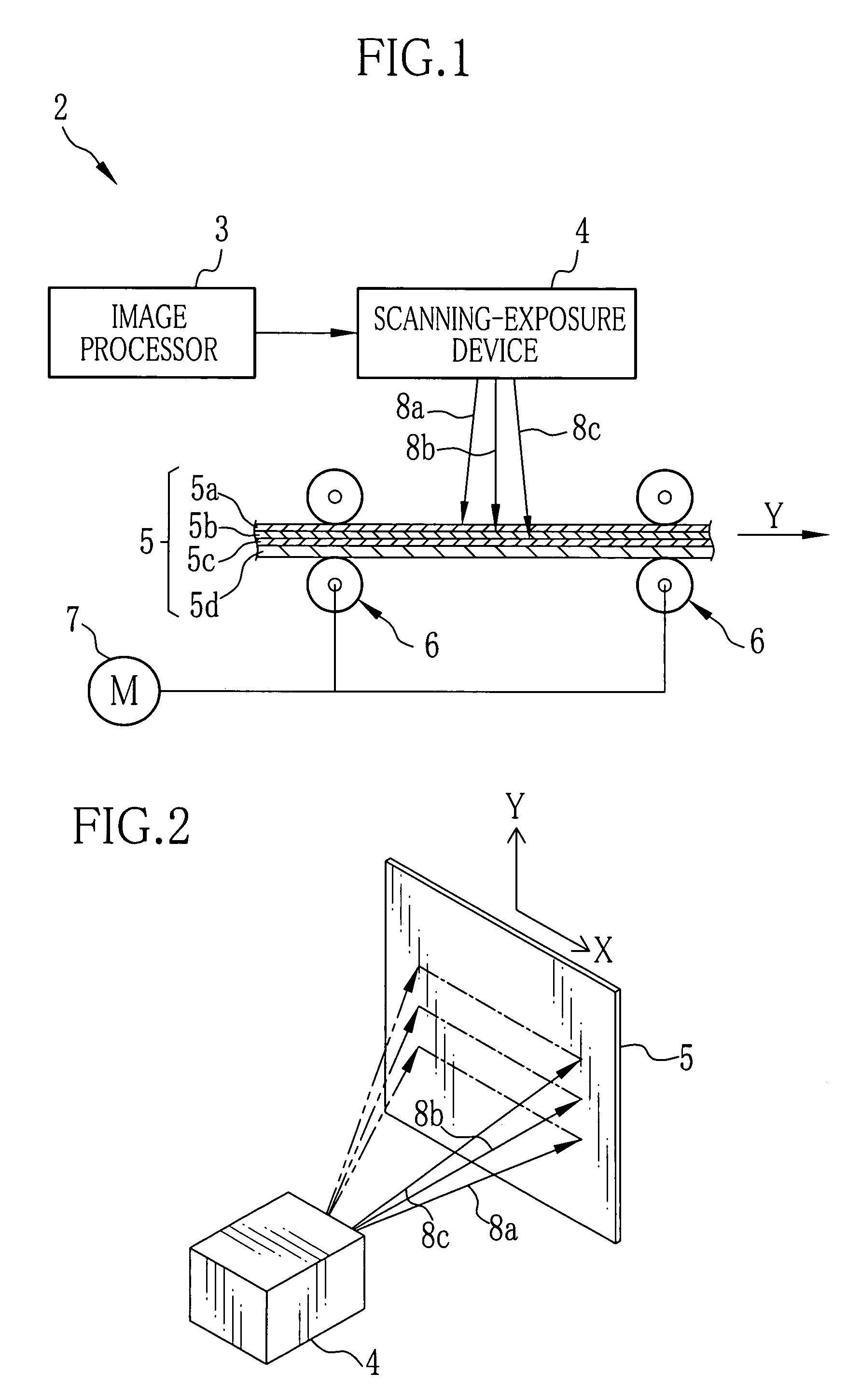
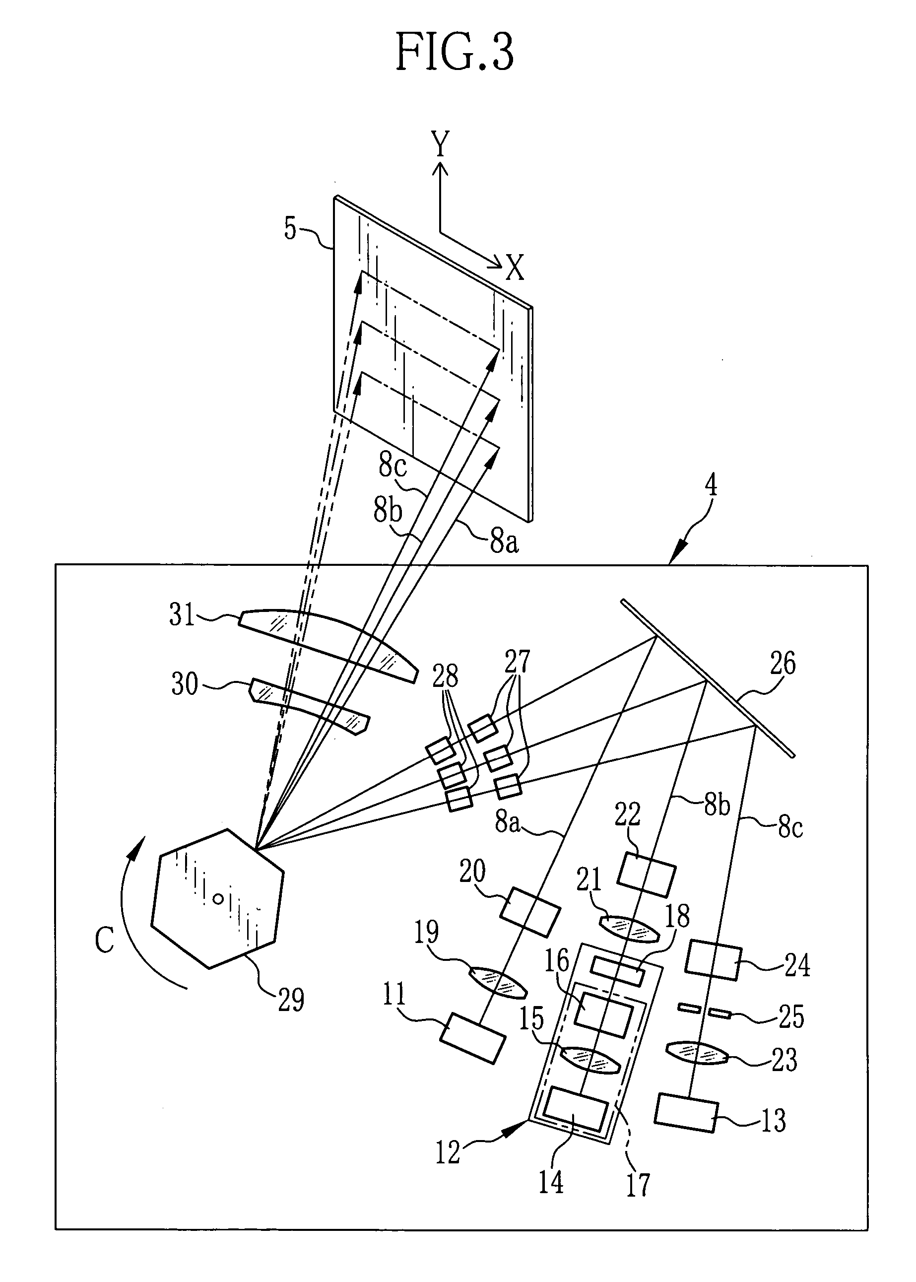
[0038]FIG. 1 shows a laser printer 2 that is constituted of an image processor 3, a scanning-exposure device 4, conveyer rollers 6 for conveying a sheet of photosensitive material 5, and a motor 7 for driving the conveyer rollers 6. The image processor 3 is fed with image data obtained by reading images from photographic film through a CCD scanner or capturing images by a digital camera. The image processor 3 processes the image data for image correction and the like to output them as image recording data.

[0039]The scanning-exposure device 4 is provided with three laser light sources that emit laser beams 8a to 8c for red, green and blue. The scanning-exposure device 4 modulates the laser beams 8a to 8c in accordance with the image recording data from the image processor 3. The modulated laser beams 8a to 8c are projected to the photosensitive material 5 while being scanned in a main scan direction X, as shown in FIG. 2. The photosensitive material 5 is a sheet having red, green and...


PUM


Abstract

A blue laser light source is a semiconductor laser having a sapphire substrate that is transparent to a wavelength of a blue laser beam emitted from an active layer. A condenser lens converges the blue laser beam at a focal point where a modulator is placed. A slit plate limits the light flux on the exit side of the condenser lens. A slit of the slit plate is located at a depth position (Z) on an optical axis of the condenser lens, and the depth position satisfies the following conditions: Z≧Z0 (Z0<0) and Pp(Z0)=P1, wherein Z is assumed to have a positive value on a forward side of the blue laser beam from the focal point, Pp(Z) is a value obtained by dividing a width of the blue laser beam in the parallel direction to the active surface at the depth position Z by a width of the extraneous light in the parallel direction at said depth position, and P1 is a convergent value of Pp(Z) at the infinity (Z→∞).

Description

FIELD OF THE INVENTION[0001]The present invention relates to a light source device for scanning-exposure and a method and an apparatus for scanning-exposure, and especially to a light source device for scanning-exposure that is provided with a flare stop for limiting light bundle to eliminate extraneous light elements called flares which are specific to any GaN semiconductor lasers.BACKGROUND ARTS[0002]As a photographic printer that records images based on image data, a laser printer using laser beams is known, wherein the laser beams is scanned across a sheet of photosensitive material in a main scan direction as the photosensitive material is conveyed in a sub scan direction orthogonal to the main scan direction. An example of the photosensitive material is of a silver-salt type, on which a latent image is recorded by the scanning-exposure, and comes up to the surface by photographic development.[0003]The laser printer is provided with a scanning-exposure apparatus that uses a lig...

Claims


Application Information

Patent Timeline
Patent Type & Authority Patents(United States)
IPC IPC(8): B41J27/00G02B9/00G02B9/08
CPCB82Y20/00G02B26/123H04N1/12H04N1/1135H01S5/34333
Inventor SAITO, KENICHIMORIMOTO, YOSHINORITANABE, TSUYOSHI
Owner FUJIFILM CORP
Why Eureka
Try Eureka