Method and apparatus to minimize power and ground bounce in a logic device

a logic device and power and ground bounce technology, applied in the direction of electric variable regulation, process and machine control, instruments, etc., can solve the problems of large power consumption of devices, large current swing of logic devices, and requiring 200 watts or more, so as to minimize logic device errors, clean power and ground voltage, and increase bypass capacitance

Active Publication Date: 2007-11-13
TEXAS INSTR INC
View PDF9 Cites 9 Cited by
  • Summary
  • Abstract
  • Description
  • Claims
  • Application Information

AI Technical Summary

Benefits of technology

[0013]A predictive power regulation apparatus is described that reduces power and ground bounce caused by the I / O buffer circuitry switching in the logic device. The apparatus includes a data storage device connected to the I / O buffer circuitry and a predictor connected to the data storage device. The data storage device may be a shift register. The apparatus also includes a voltage or current smoothing device connected to the predictor, the voltage or current smoothing device providing adjusted voltage or current to power and ground planes of the logic device.
[0014]The predictive power regulation apparatus can minimize power and ground bounce in a logic device by predicting the next state of input / output buffer circuitry in the logic device. In some embodiments of the invention, the apparatus determines a current requirement of the logic device to switch the I / O buffer circuitry to its next state. After determining the current requirement, the apparatus adjusts current on the power and ground planes of the logic device to the required current during switching of the I / O buffer circuitry to its next state. The current on the power and ground planes of the logic device is adjusted by increasing or decreasing the current to the determined value at start of switching of the I / O buffer circuitry to its next state. The current on the power and ground planes of the logic device is adjusted by holding the current at a steady state value corresponding to voltage Vdd after the input / output buffer circuitry has completed switching to its next state.
[0016]A method of minimizing power and ground bounce in a logic device is described that includes predicting from a list of instructions in a buffer the next instruction to be executed by the logic device. The logic device contains power and ground planes. A current requirement of the logic device to execute the instruction is determined. The current on the power and ground planes of the logic device is adjusted to the determined current requirement for executing the instruction.
[0018]The present invention provides significant advantages over the prior art. One advantage is a clean power and ground voltage and current that minimizes error on the logic device. Thus, a new package structure with increased bypass capacitance and low inductive load close to the logic device is not needed for reducing power and ground bounce. Another advantage is that the apparatus and method can be used with logic devices of any number of transistors and power consumption without significant redesign of the logic device and the apparatus and method itself.

Problems solved by technology

Such devices consume large amounts of power, requiring 200 watts or more.
Software instructions executing on the logic device can cause vast swings in the current needed by the logic device.
As a result of the resistance and inductance in the power and ground planes and buses, these large current draws can result in voltage noise that can lead to malfunction of the logic device.
However, high performance logic devices such as microprocessors may require upwards of 30 amperes of current for various subsystems.
Such high currents and corresponding voltages cannot easily be filtered by the bypass capacitors to minimize power and ground bounce.
The techniques described above require complex and time consuming design of the logic device circuitry and do not eliminate the power and ground bounce.

Method used


Image

  • Method and apparatus to minimize power and ground bounce in a logic device
  • Method and apparatus to minimize power and ground bounce in a logic device
  • Method and apparatus to minimize power and ground bounce in a logic device

Examples


Embodiment Construction

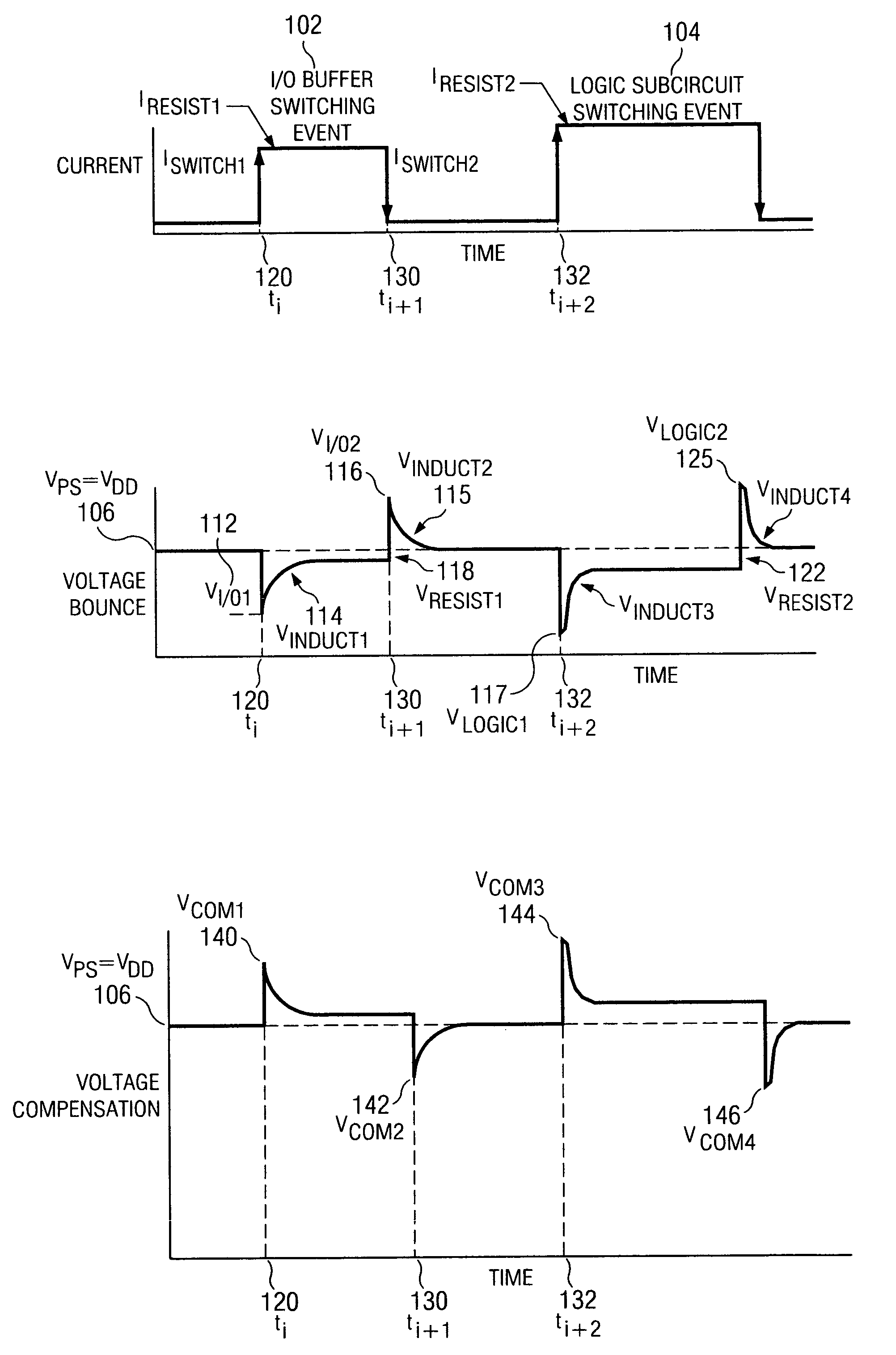
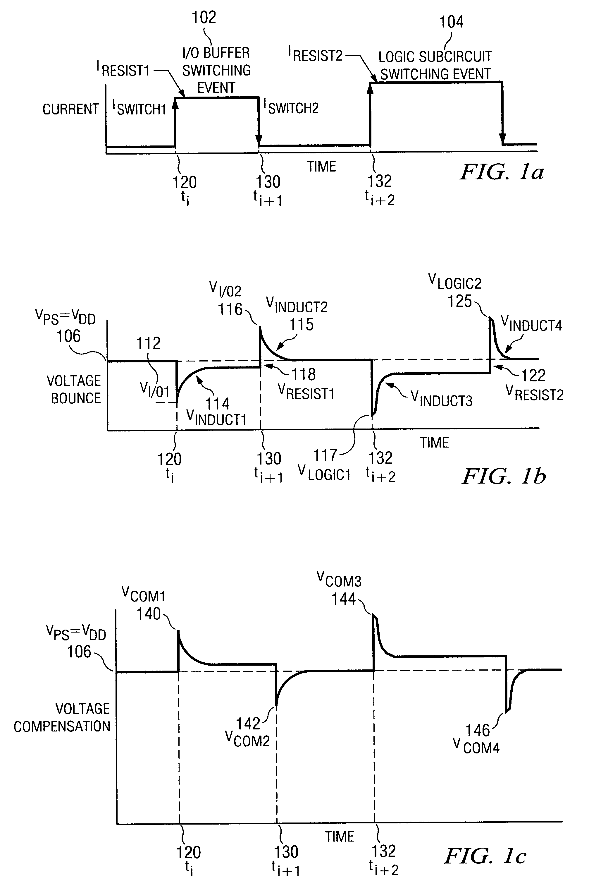
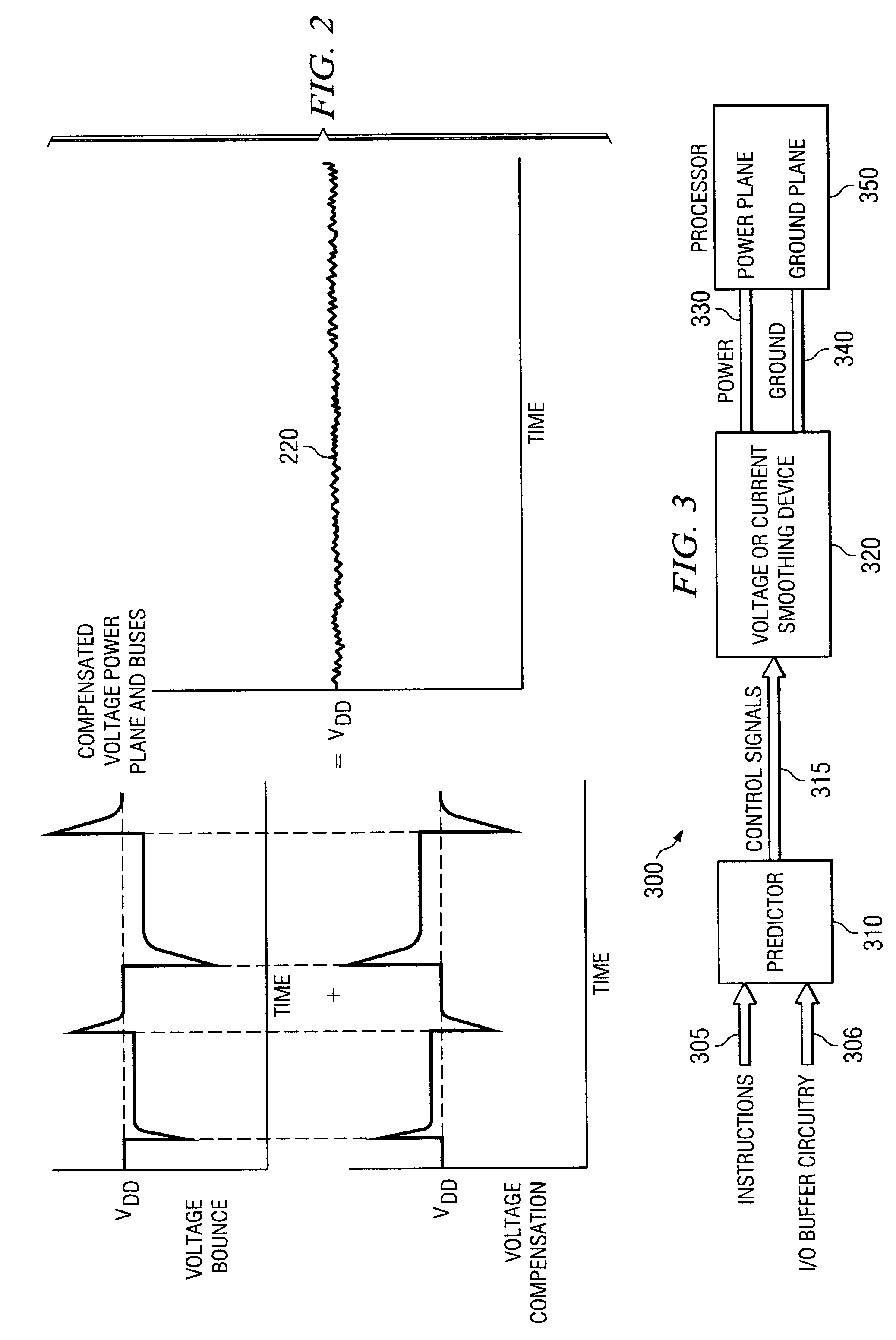
[0031]FIG. 1a shows a graph of current versus time for two switching events in a logic device. During first switching event 102, I / O buffer circuitry in the logic device switching states from binary zero to one or binary one to zero may cause the current to stay on from ti 120 to ti+1 130. The rise of the current at ti 120 and fall of the current at ti+1 130 can result in the voltage bounce shown in FIG. 1b. Second switching event 104, may be caused by the subcircuits of the logic device switching on and off to execute instructions. The rise of the current at time ti+2 132 and fall of the current at ti+3 133 because of subcircuit switching event 104 can also result in voltage bounce as shown in FIG. 1b. As shown in FIG. 1a, logic subcircuit switching event 104 may require current of a greater magnitude than I / O buffer switching event 102 resulting in the voltage bounce shown in FIG. 1b for the logic subcircuit switching event being of greater magnitude than the bounce from the I / O b...


PUM


Abstract

A predictive power regulation apparatus and method that minimizes power and ground bounce in a logic device. The apparatus includes a predictor and a voltage or current smoothing device connected to the predictor. The voltage or current smoothing device outputs adjusted voltage or current to power and ground planes of the logic device. In one embodiment, the predictor includes an instruction scanner device and a look-up table connected to the instruction scanner device. The instruction scanner device determines the next instruction to be executed by the logic device. A voltage / current scheduling buffer connected to the look-up table contains voltage and current compensation and the time at which the voltage or current compensation should be requested from the voltage or current smoothing device. An alternative predictive power regulation apparatus is described that reduces power and ground bounce caused by the I / O buffer circuitry switching in the logic device.

Description

[0001]This application claims priority under 35 USC § 119(e)(1) of Provisional Application No. 60 / 529,072, filed Dec. 13, 2003.FIELD OF THE INVENTION[0002]The present invention generally relates to reducing voltage swing in integrated circuits. More particularly, the invention relates to minimizing voltage fluctuations on the power and ground planes of integrated circuit chips. Still more particularly, the invention relates to predicting the voltage or current needed at a future time by a processor in order to minimize voltage bounce on the power and ground planes.BACKGROUND OF THE INVENTION[0003]Logic devices such as digital signal processors, microprocessors, programmable circuit devices, and Application Specific Integrated Circuits (ASICs) contain many millions of transistors switching at very high frequencies. Such devices consume large amounts of power, requiring 200 watts or more. Power P may be defined as the voltage V between the power and ground buses of a logic device mult...

Claims


Application Information

Patent Timeline
Patent Type & Authority Patents(United States)
IPC IPC(8): G06F1/26H03K19/003
CPCH03K19/00369
Inventor EDWARDS, DARVIN R.
Owner TEXAS INSTR INC
Why Eureka
Try Eureka