System and method for point-of-use filtration and purification of fluids used in substrate processing

a technology of point-of-use filtration and purification of fluids used in substrate processing, which is applied in the direction of filtration separation, multi-stage water/sewage treatment, separation process, etc., can solve the problems of increasing the probability of device failure, contaminating particle or impurity on a wafer occupying a greater percentage of the device's surface area, and increasing the likelihood of device failure, etc., to reduce or eliminate particles and/or ionic impurities in fluid

Active Publication Date: 2007-12-25
AKRION TECH
View PDF7 Cites 10 Cited by
  • Summary
  • Abstract
  • Description
  • Claims
  • Application Information

AI Technical Summary

Benefits of technology

[0017]It is, therefore, an object of the present invention to provide a system and method to reduce or eliminate particles and / or ionic impurities in fluids used to process substrates.
[0018]Another object of the present invention is to provide a system and method of reducing or eliminating particles and / or ionic impurities in fluids used to process substrates that removes trace metals from the fluids without injecting chemicals into the fluids, such as hydrochloric acid.
[0019]Yet another object of the present invention is to provide a system and method of reducing or eliminating particles and / or ionic impurities in fluids used to process substrates that continuously monitors / measures the amount of particles and / or ionic impurities in the fluids in real time during substrate processing.

Problems solved by technology

Moreover, as semiconductor devices become more miniaturized and complex due to end product needs, the cleanliness requirements have become more stringent.
First, as devices become miniaturized, a contaminating particle or impurity on a wafer will occupy a greater percentage of the device's surface area.
This increases the likelihood that the device will fail.
Second, as devices become more complex, the raw materials, time, equipment, and processing steps necessary to make these devices also become more complex and more expensive.
As a result, the cost required to make each wafer increases.
These fluids often carry contaminants, such as particles and ionic impurities.
Thus, the process fluids themselves can act to contaminate the wafers and decrease yield by carrying contaminants to the wafer surfaces.
Even if pure water leaves the central facility, bacteria growing in the pipes can enter the rinsing system, and contaminate the wafers.
Thus, even if the rinse water is typically filtered by the DI water making plant, the particle counts are still high enough to negatively impact the quality of the wafer cleaning results because these liquid-borne particles will deposit onto the wafers when exposed to the DI water.
Operating a clean air and water distribution networks throughout the foundry presents an economic problem.
The cost of operating a cleaning facility is related to the degree of cleanliness and the volume of water required.
Because only a relatively small amount of air and water needs to be of the highest purity, this may result in an unduly expensive central water purification system.
Additionally, even if DI water plants usually produce ultra pure DI water some contamination still takes place, for example, during the change of the resin beds.
In such a centralized system, however, wafers cannot be produced while the system is being purged, causing production delays and shutdown of some operations.
Consequently, such steps may be taken only when contamination problems become known to the operators.
This exposes the wafers to significant levels of impurities in the water between the system purges.
Process fluid contamination problem also arise in process chambers utilizing recirculating systems.
In such systems pumps and any other moving parts in the loop can be the major contributors of contamination.
Moreover, because the same process fluid is being recirculated back into the process chamber after contacting (and processing) wafers, contaminants, including particles, metals, photoresist, etc., that are removed from the wafers can be reintroduced back into the process chamber and contaminate the wafers.
However, the Mohindra et al. system is less than optimal for a number of reasons.
First, the filter bank of the Mohindra et al. system only removes contaminants that are about 0.1 microns (μm) or larger.
With the devices on wafers becoming even more miniaturized, contaminants that are smaller than 0.1 m can negatively impact yield.
Thus, the Mohindra et al. system will not meet industry needs.
Moreover, the filter bank of the Mohindra et al. system disclosed in the '043 patent does not sufficiently remove metallic ionic impurities from the fluids.
The process and apparatus required to inject chemicals / acids into the fluid stream to remove metals have the disadvantage of containing moving parts, inaccurate dispense, and possible malfunctioning.
As such, the process fluid may contain unacceptable amounts of contaminants and the user may continue to process wafers until yield issues and / or defects in the devices come to light somewhere along the production line.
This can expose many wafers to unfavorable processing conditions resulting in many wafers being ruined, thereby resulting in substantial economic detriment.

Method used


Image

  • System and method for point-of-use filtration and purification of fluids used in substrate processing
  • System and method for point-of-use filtration and purification of fluids used in substrate processing
  • System and method for point-of-use filtration and purification of fluids used in substrate processing

Examples


Embodiment Construction

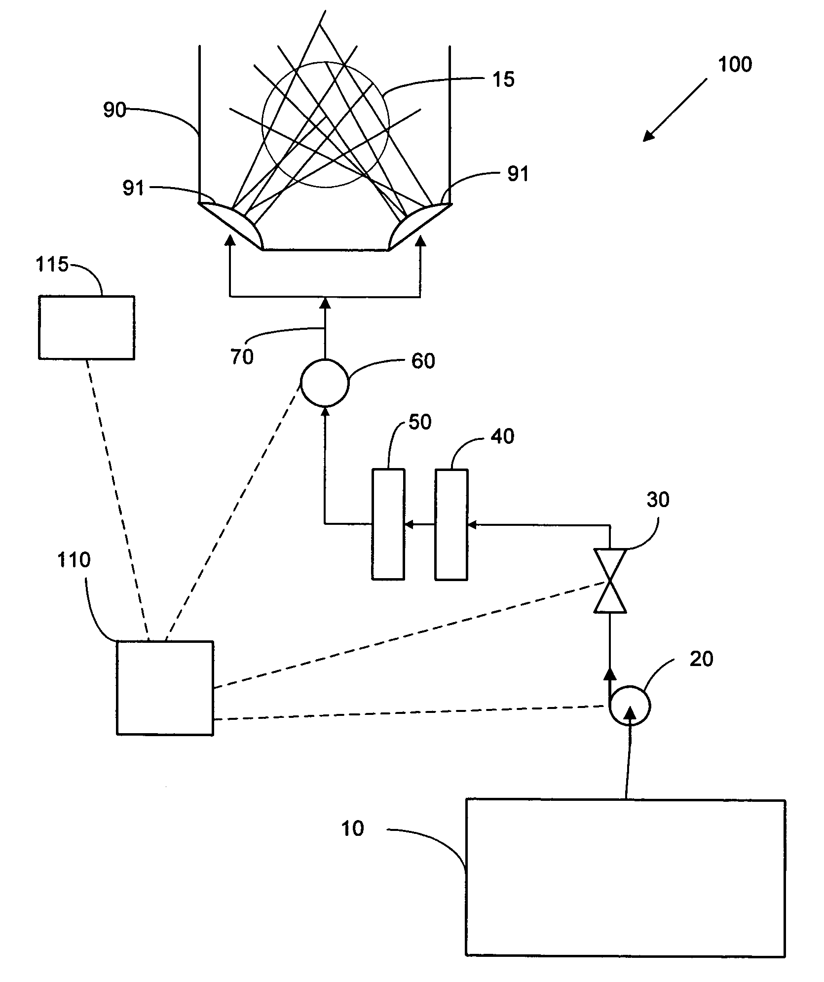
[0045]FIG. 1 illustrates a schematic of point-of-use filtration and purification (“POUFP”) rinse system 100 in accordance with an embodiment of the present invention. While the system (and method) are described in detail with respect to a semiconductor DI water rinsing system, the invention is not so limited. The inventive system and method can be used to filter and purify any type of fluid that is used to process substrates, including but not limited to chemicals, acids, liquid-liquid mixtures, diluted chemistries, and liquid-gas solutions. The system and method is also not limited to supplying ultra-pure fluid for semiconductor wafer processing but can be used with any type of substrate processing where ultra-pure fluid is desired, such as the manufacture of raw wafers, lead frames, medical devices, disks and heads, flat panel displays, microelectronic masks, and other applications requiring high purity fluids for processing.

[0046]POUFP rinse system 100 comprises DI water reservoi...


PUM

PropertyMeasurementUnit
sizeaaaaaaaaaa
sizesaaaaaaaaaa
sizesaaaaaaaaaa

Abstract

A method and system for supplying an ultra-pure fluid to a substrate process chamber using point-of-use filtration and purification. The method and system provide ability to automatically monitor and control contamination levels in fluids in real time and to stop substrate processing when contamination levels exceed predetermined thresholds. In one aspect, the invention is a system comprising: a fluid supply line adapted to supply a fluid to the process chamber; filtration means operably coupled to the fluid supply line for removing positively and negatively charged particles from the fluid prior to the fluid passing into the process chamber; a purifier operably coupled to the fluid supply line in series with the filtration means for removing ionic contaminants from the fluid prior to the fluid passing into the process chamber; sensor means for repetitively measuring particle and ionic impurity levels in the fluid that has passed through the filtration means and the purifier, the sensor means producing signals indicative of the measured particle and ionic impurity levels; a controller electrically coupled to the sensor means for receiving the signals created by the sensor means, the controller adapted to respectively compare the measured particle level and the measured ionic impurity level indicated by the signals to a predetermined particle threshold and a predetermined ionic impurity threshold, wherein upon the controller determining that either the measured particle level is above the predetermined particle threshold and / or that the measured ionic impurity level is above the predetermined ionic impurity threshold, the controller further adapted to (1) activate means to alert a user, (2) cease processing of substrates in the process chamber, and / or (3) prohibit processing of substrates in the process chamber.

Description

CROSS-REFERENCE TO RELATED APPLICATIONS[0001]The present application claims the benefit of U.S. Provisional Patent Application, Ser. No. 60 / 489,059, filed Jul. 21, 2003, the contents of which are fully incorporated herein by reference.FIELD OF THE INVENTION[0002]The present invention relates generally the field of semiconductor integrated circuit processing, and specifically to systems and methods of supplying pure fluids to substrates, such as semiconductor wafers, for processing. However, the invention can also be applied to the manufacture of raw wafers, lead frames, medical devices, disks and heads, flat panel displays, microelectronic masks, and other applications requiring high purity fluids for processing.BACKGROUND OF THE INVENTION[0003]In the manufacture of semiconductors, semiconductor devices are produced on thin disk-like objects called wafers. Generally, each wafer contains a plurality of semiconductor devices. The importance of minimizing contaminants on the surface of...

Claims


Application Information

Patent Timeline
Patent Type & Authority Patents(United States)
IPC IPC(8): B01D1/00C02F1/00C02F1/42C02F1/44C02F1/58C02F9/00H01L21/00
CPCC02F9/005C02F1/42C02F1/444C02F2103/04H01L21/67057C02F2209/006C02F2209/05C02F2209/10H01L21/67051C02F2209/005C02F9/20
Inventor KASHKOUSH, ISMAIL
Owner AKRION TECH
Why Eureka
Try Eureka