
Configurable integrated circuit with built-in turns

a technology of integrated circuits and turns, applied in the direction of computation using denominational number representation, instruments, pulse techniques, etc., can solve the problems of inefficiency and high cost of connection architecture illustrated in fig. 2, not designed to optimize the number, and undesirable cycles

Inactive Publication Date: 2007-12-25
ALTERA CORP
View PDF79 Cites 21 Cited by
  • Summary
  • Abstract
  • Description
  • Claims
  • Application Information

AI Technical Summary

Benefits of technology

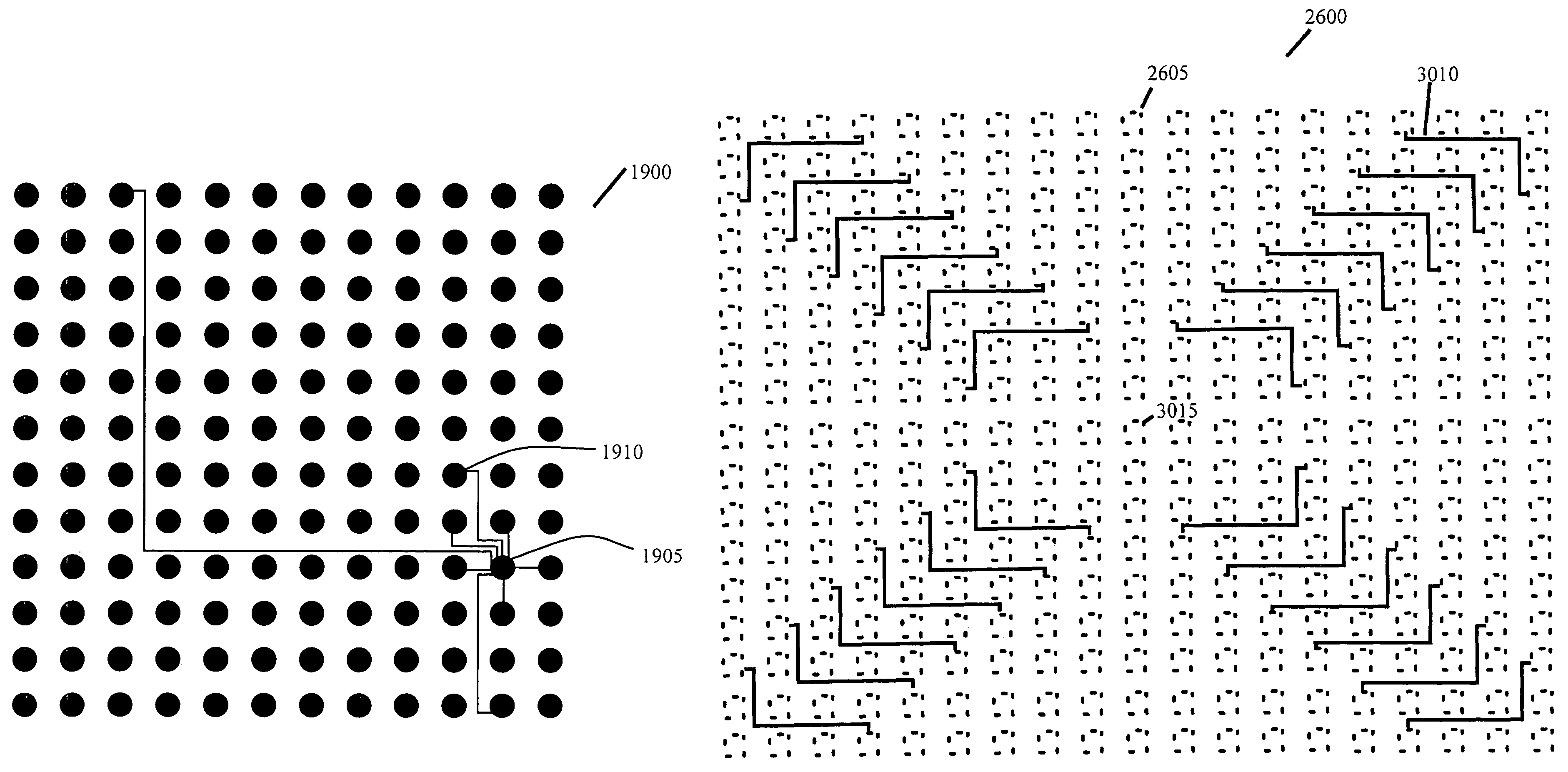
The invention provides configurable integrated circuits (ICs) with configurable node arrays. These arrays have numerous nodes arranged in rows and columns, with direct offset connections between nodes. The connections can involve wire segments and vias, and some connections have intervening circuits. The ICs also have two similar nodes within the array and two different connection schemes. The method identifies different sets of connections and computes a metric score for each set to select the best connection scheme for the nodes. The technical effect is the ability to create highly customizable ICs with complex node arrays and direct offset connections.

Problems solved by technology

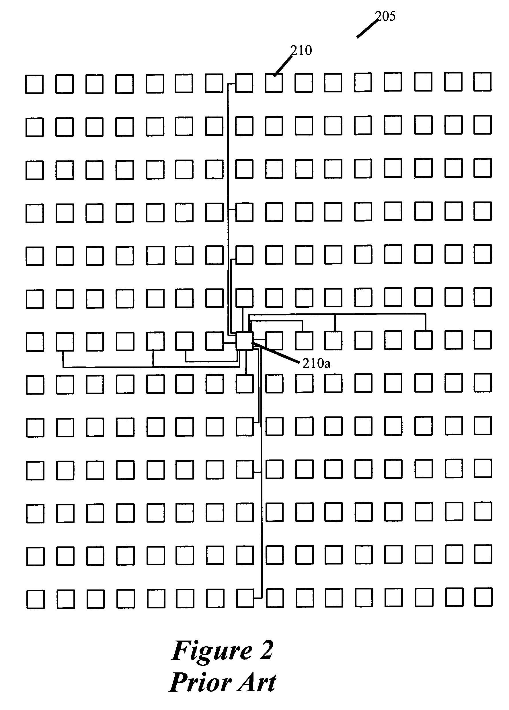
This requirement makes the connection architecture illustrated in FIG. 2 inefficient and expensive as each connection requires the use of transistor switching logic.
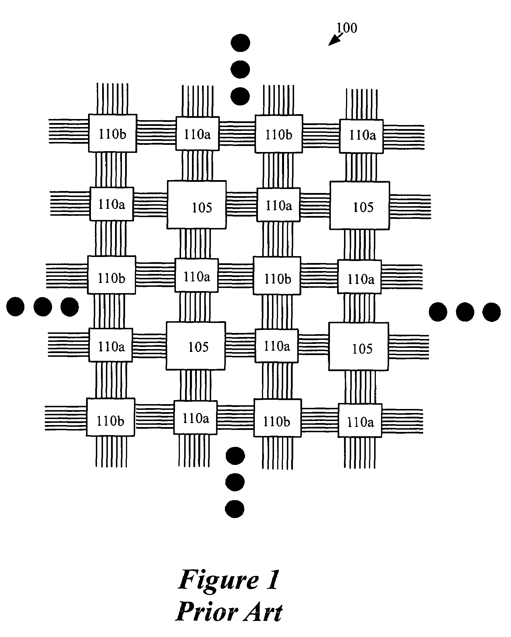
Also, the connection architecture illustrated in FIG. 2 is not designed to optimize the number of CLB's reachable from any given CLB.
Such cycles are undesirable as they come at the expense of reachability of other CLB's.
The uniform connection architecture of FIG. 2 is also inefficient as it provides more ways than necessary for reaching one CLB from another CLB.
This redundancy is undesirable as it comes at the expense of reachability of other CLB's.

Method used


Image

  • Configurable integrated circuit with built-in turns
  • Configurable integrated circuit with built-in turns
  • Configurable integrated circuit with built-in turns

Examples


Embodiment Construction

[0040]In the following description, numerous details are set forth for purpose of explanation. However, one of ordinary skill in the art will realize that the invention may be practiced without the use of these specific details. For instance, not all embodiments of the invention need to be practiced with the specific number of bits and / or specific devices (e.g., multiplexers) referred to below. In other instances, well-known structures and devices are shown in block diagram form in order not to obscure the description of the invention with unnecessary detail.

I. Definitions

[0041]A logic circuit is a circuit that can perform a function on a set of input data that it receives. A configurable logic circuit is a logic circuit that can be configured to perform different functions on its input data set. FIG. 4 illustrates an example of a configurable logic circuit 400 that can perform a set of functions. As shown in this figure, the logic circuit 400 receives a set of input data 410 and a ...


PUM


Abstract

Some embodiments provide a configurable integrated circuit (“IC”) with a configurable node array. A configurable node array may include configurable nodes arranged in rows and columns. It may also include direct offset connections, with each direct offset connection connecting two nodes that are neither in the same column nor the same row. In some embodiments, at least some direct offset connections connect pairs of nodes that are separated by more than one row and at least one column, or by more than one column and at least one row. Some embodiments establish a direct connection by a set of wire segments that traverse through a set of the IC's wiring layers, and a set of vias when multiple wiring layers are involved. Some of the direct connections may have intervening circuits (e.g. buffer circuits). In some embodiments, the nodes in the array are all similar to each other.

Description

CROSS REFERENCE TO RELATED APPLICATIONS[0001]This application is related to the following applications with the same filing date: U.S. patent application Ser. No. 10 / 882,713 filed on Jun. 30, 2004; U.S. patent application Ser. No. 10 / 882,848 filed on Jun. 30, 2004; and U.S. patent application Ser. No. 10 / 883,502 filed on Jun. 30, 2004.FIELD OF THE INVENTION[0002]The present invention is directed towards configurable integrated circuit with built-in turns.BACKGROUND OF THE INVENTION[0003]The use of configurable integrated circuits (“IC's”) has dramatically increased in recent years. One example of a configurable IC is a field programmable gate array (“FPGA”). An FPGA is a field programmable IC that has an internal array of logic circuits (also called logic blocks) that are connected together through numerous interconnect circuits (also called interconnects). In an FPGA, the internal array of logic and interconnect circuits is typically surrounded by input / output blocks. Like some oth...

Claims


Application Information

Patent Timeline
Patent Type & Authority Patents(United States)
IPC IPC(8): G06F7/38H01L25/00H03K19/173H03K19/177
CPCH03K19/17796H03K19/17736
Inventor ROHE, ANDRETEIG, STEVEN
Owner ALTERA CORP
Learn More