

Apparatus, system, and method for junction isolation of arrays of surface emitting lasers
a laser array and surface technology, applied in semiconductor lasers, instruments, optics, etc., can solve the problems of reducing efficiency, affecting the efficiency of array interconnection schemes, and non-uniform light outpu
- Summary
- Abstract
- Description
- Claims
- Application Information
AI Technical Summary
Problems solved by technology
Method used
Image

Examples
Embodiment Construction
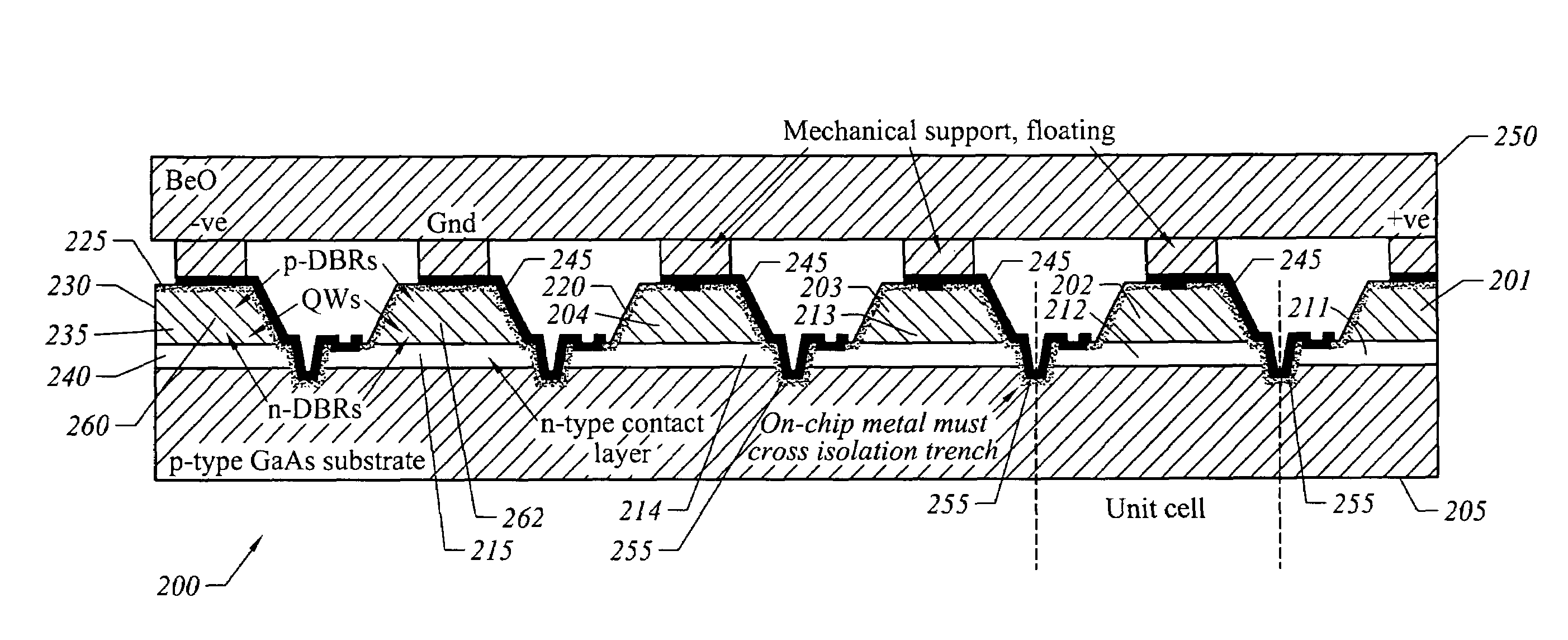
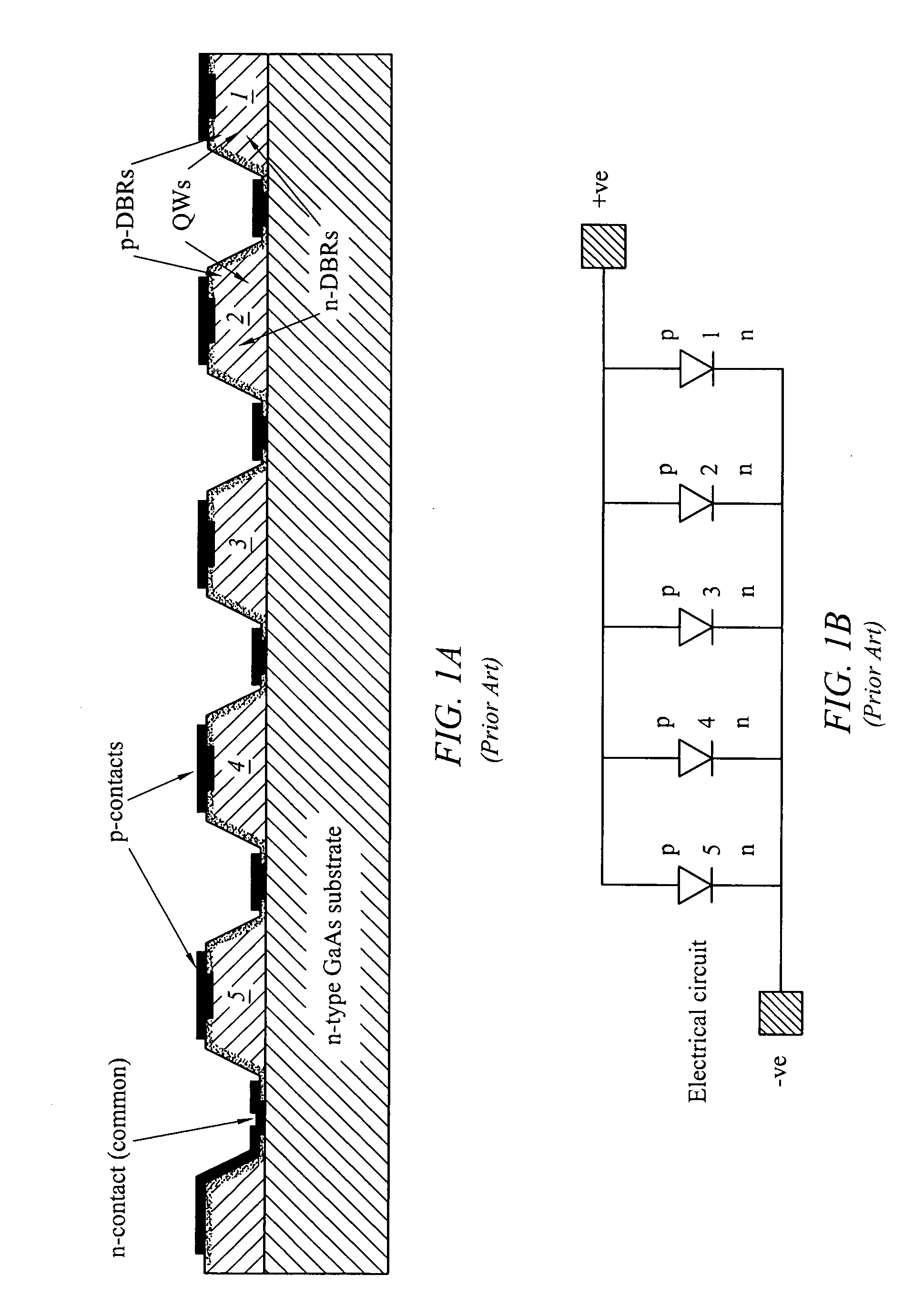
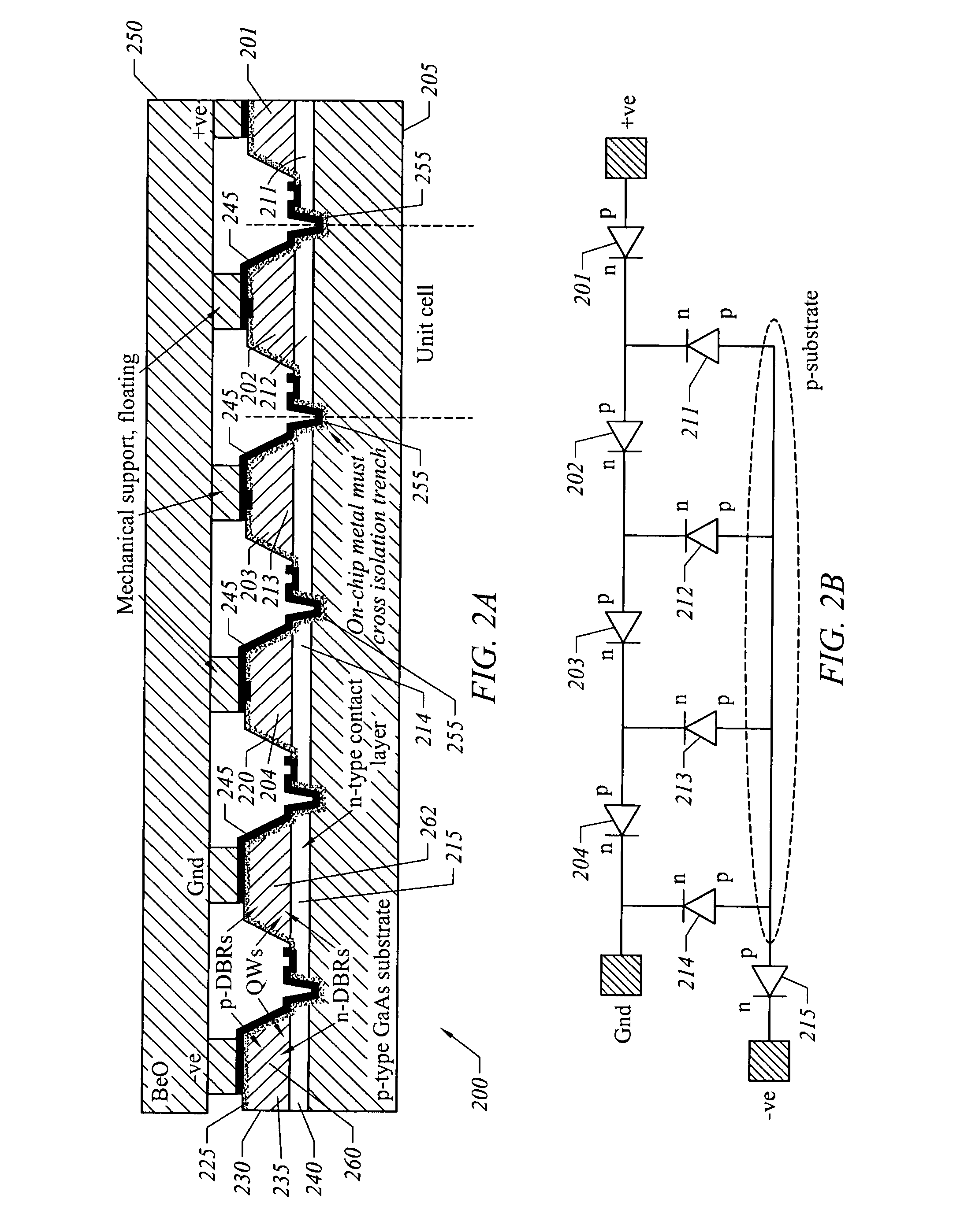
[0029]FIG. 2A illustrates an array of surface emitting laser diodes 201, 202, 203, and 204 formed on a p-type substrate 205 of a common die 200. Throughout the following discussion it will be understood that doping types are exemplary and that inverting the polarity of the doping types and corresponding operating voltages results in electrical devices having similar equivalent circuits and principles of operation.
[0030]Each laser diode 201, 202, 203, and 204 has a top p-type contact layer 220, p-type laser diode region 225 (e.g., a p-type distributed Bragg reflector (DBR), active region 230, n-type laser diode region 235 (e.g., a n-type DBR), and a bottom n-type contact layer 240. The bottom n-type contact layer 240 has a doping-thickness product selected to provide a low-resistance connection to an individual laser diode. In one implementation the bottom n-type contact layer 240 is approximately five to ten microns thick and is a moderate-to heavily-doped n-type layer that is grown...
PUM
 Abstract
Description
Claims
Application Information