High productivity plasma processing chamber

a plasma processing chamber and high-efficiency technology, applied in the direction of coatings, chemical vapor deposition coatings, electric discharge tubes, etc., can solve the problems of shortened life of critical chamber components, more downtime, and chamber downtime, so as to minimize the entry of process products, reduce the entry rate, and maximize the allowable time

Inactive Publication Date: 2005-10-20
APPLIED MATERIALS INC
View PDF7 Cites 368 Cited by
  • Summary
  • Abstract
  • Description
  • Claims
  • Application Information

AI Technical Summary

Benefits of technology

[0016] The present invention includes apparatus and methods for maximizing the allowable time between in-situ cleans of a plasma processing chamber by reducing the rate at which process products accumulate onto or attack surfaces inside the chamber. The apparatus includes a reduced gap between the process chamber and the substrate support to minimize entry of process products into the lower chamber and subsequent deposition on chamber surfaces. The apparatus further includes temperature control systems for the showerhead—both heating and cooling—to minimize temperature fluctuations and a heating system for the chamber body to ameliorate unwanted deposition of process products in the lower chamber. The apparatus further includes an insert between the chamber lid support and isolator for better thermal isolation of the isolator as well as reducing temperature gradients inside the isolator. The methods include controlling the temperature of the showerhead and chamber walls to constant, optimal temperatures. The methods also include pressurizing the lower chamber with a purge gas to prevent entry of process products.

Problems solved by technology

However, the increasingly stringent substrate-processing requirements that improve semiconductor device yield often lead to more downtime.
Also contributing to chamber downtime is the shortened lifetime of critical chamber components.
This is brought about by outright failure of the components or simply their inability to function as required after prolonged use in the severe environment of a process chamber.
Repeated exposure to high temperatures and highly reactive process chemicals can alter a component's critical dimensions through deformation or erosion, or,cause it to fail catastrophically.
Even minor warping or other changes in the shape of some process chamber components can have a serious effect on the uniformity of a deposited film on a substrate.
High particle counts detected on substrates result in additional chamber downtime while the cause is determined and corrected.
Over time, the deposited byproducts or the corroded or pitted chamber surfaces tend to release particles, resulting in particle defects on substrates being processed in the chamber.
This is particularly true where high-pressure plasma processes or high plasma powers are utilized during the semiconductor fabrication process; the processing gases and / or generated plasma are more prone to leak out of the processing region of the chamber and form deposits.
Also, these deposits are much more likely-to flake off or generate particles when the surface they are deposited on is subject to large oscillations in temperature.
But adding components inside a processing chamber has drawbacks, increasing chamber cost and internal surface area.
Greater surface area in a processing chamber lengthens chamber pump-down time prior to processing, increasing process chamber downtime.
Also, while shielding does protect a chamber's internal components from reactive process gases and deposits, it does not prevent the accumulation of process products on the shielding itself.
Therefore, deposits of process byproducts will still be a source of particle contamination in the processing chamber.
However, the in-situ chamber clean is conducted as infrequently as possible since it prevents devices from being processed and therefore is defined as downtime.
Another contributor to chamber downtime is replacement of process chamber components due to wear and tear or because of unexpected failures of the components.
One component that is subject to failure is the heater assembly of plasma-processing chamber as well as many of this assembly's constituent parts.
In addition to being a relatively expensive component, a heater assembly is time consuming to replace, so any increase in its reliability will positively impact chamber down-time.
Aluminum heater pedestals provide high heating and plasma uniformity and greater heater element reliability, but are prone to deformation that ultimately reduces uniformity; at process temperatures aluminum is not strong enough to remain completely rigid and over time pedestals sag and warp.
Also, the non-uniform arrangement of the heater elements inside the pedestal creates hotter and cooler regions, causing warping of the pedestal.
Ceramic heater pedestals are rigid at process temperatures, but have higher cost and provide poor heating and plasma uniformity relative to aluminum heaters.
Mechanical fatigue of such heating elements at the feed-through point is a common failure mechanism for pedestal heaters.
When the vacuum seal for the electrical connections is in close proximity to the heater, finding a material that reliably meets the above requirements for such a seal is problematic.
Because neither the substrate nor the pedestal surface can be manufactured to be perfectly flat, the substrate will only contact the surface of the pedestal at a few discrete points, therefore undergoing uneven heating.
These rest points or features on the face of the heater pedestal are subject to wear after large numbers of substrates have been processed on the heater pedestal.
Replaceable—and therefore removable—rest points can be used, but add significant complexity to the design of the pedestal.
Threaded fasteners introduce the potential for creating dead volumes inside the plasma-processing chamber.

Method used


Image

  • High productivity plasma processing chamber
  • High productivity plasma processing chamber
  • High productivity plasma processing chamber

Examples


Embodiment Construction

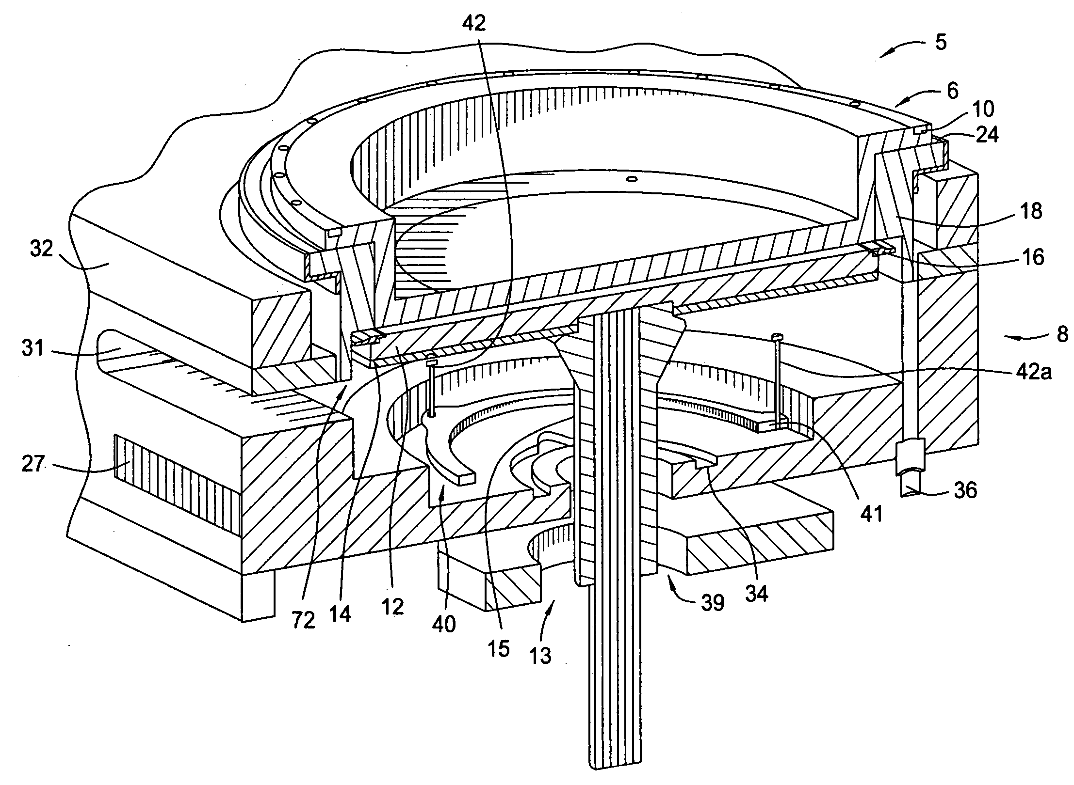
[0034] Embodiments of the present invention generally relate to apparatus and methods for an improved semiconductor plasma-processing chamber.

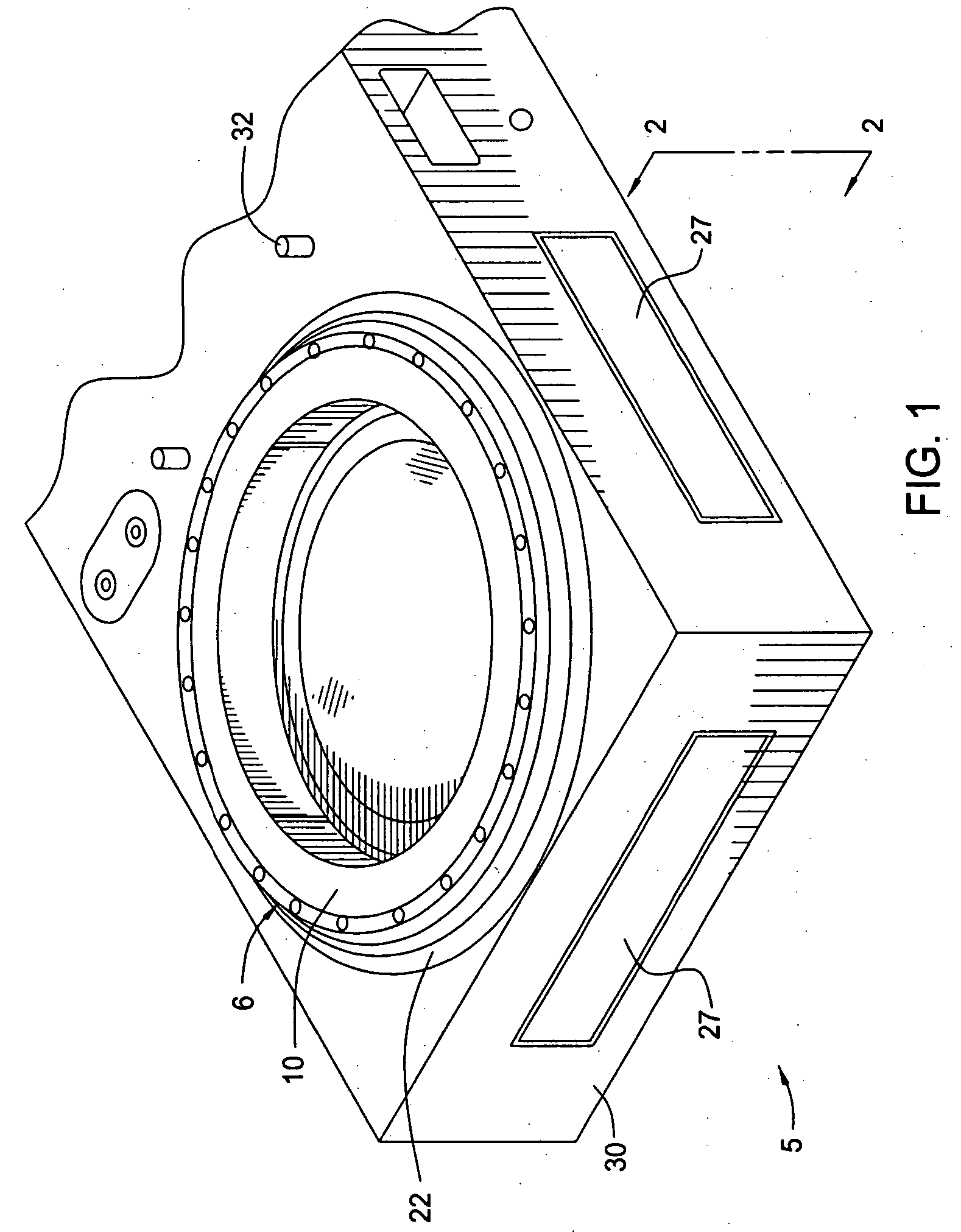
[0035]FIG. 1 illustrates a single substrate plasma-processing chamber 5, which incorporates an embodiment of the present invention. The top assembly typical of such a chamber is not shown for clarity. The top assembly includes RF source, gas distribution assembly, gas boxes, and remote plasma source.

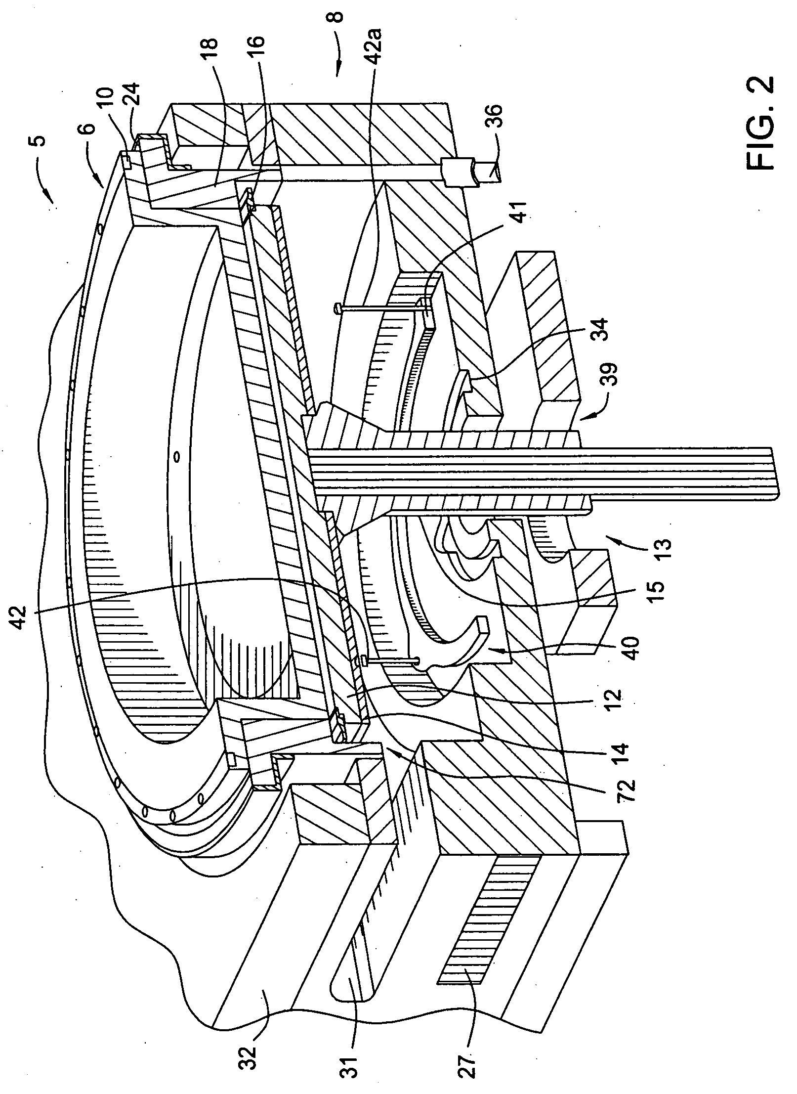
[0036] The chamber body 30 of plasma-processing chamber 5 is attached to a mainframe (not shown) that contains a wafer transport system (not shown) and system supporting hardware (not shown). The mainframe and system supporting hardware are designed to transfer the substrate under vacuum from one area of the substrate processing system, deliver the substrate to plasma-processing chamber 5 and remove the substrate when the process steps in plasma-processing chamber 5 are complete. A slit valve opening 31 (see FIG. 2) is provided for passing a subs...


PUM

PropertyMeasurementUnit
poweraaaaaaaaaa
poweraaaaaaaaaa
power ratingaaaaaaaaaa

Abstract

Embodiments of the present invention are generally directed to apparatus and methods for a plasma-processing chamber requiring less maintenance and downtime and possessing improved reliability over the prior art. In one embodiment, the apparatus includes a substrate support resting on a ceramic shaft, an inner shaft allowing for electrical connections to the substrate support at atmospheric pressure, an aluminum substrate support resting on but not fixed to a ceramic support structure, sapphire rest points swaged into the substrate support, and a heating element inside the substrate support arranged in an Archimedes spiral to reduce warping of the substrate support and to increase its lifetime. Methods include increasing time between in-situ cleans of the chamber by reducing particle generation from chamber surfaces. Reduced particle generation occurs via temperature control of chamber components and pressurization of non-processing regions of the chamber relative to the processing region with a purge gas.

Description

CROSS-REFERENCE TO RELATED APPLICATIONS [0001] This application claims benefit of U.S. provisional patent application Ser. No. 60 / 544,574, filed Feb. 13, 2004, which is herein incorporated by reference.BACKGROUND OF THE INVENTION [0002] 1. Field of the Invention [0003] Embodiments of the present invention generally relate to a semiconductor device or flat panel display processing chamber. [0004] 2. Description of the Related Art [0005] Due to competitive pressures to reduce device cost in the semiconductor and flat panel device fabrication industries, the need for both improved device yields and reduced processing chamber downtime i.e., the time that a chamber is unavailable for processing, has become important. However, the increasingly stringent substrate-processing requirements that improve semiconductor device yield often lead to more downtime. This is due in part to the narrow acceptable range of process variation for a chamber during operation. To monitor different aspects of ...

Claims


Application Information

Patent Timeline
Patent Type & Authority Applications(United States)
IPC IPC(8): C23C16/00C23C16/44C23C16/458H01J37/32
CPCC23C16/4404H01J2237/022H01J37/32522C23C16/4586H01L21/205H01L21/3065
Inventor SILVETTI, MARIO DAVIDQUACH, DAVID H.KIM, BOK HOENNOWAK, THOMASCHO, THOMAS K.HARIZ, FRED H.MOORE, ROBERT B.
Owner APPLIED MATERIALS INC
Why Eureka
Try Eureka