Multi-chip programmable logic device having configurable logic circuitry and configuration data storage on different dice

a logic circuit and configuration data technology, applied in the direction of instruments, computations using denominational number representation, pulse techniques, etc., can solve the problems of low yield of such large devices, difficult to produce large complex integrated circuits without defects, limited maximum size of fpga integrated circuits, etc., to achieve the effect of increasing the die area usable for configurable logic and improving the yield of each of these di

Inactive Publication Date: 2005-07-12
XILINX INC
View PDF36 Cites 351 Cited by
  • Summary
  • Abstract
  • Description
  • Claims
  • Application Information

AI Technical Summary

Benefits of technology

[0006]The circuitry of a programmable logic device (for example, an FPGA) includes a configurable logic portion and a configuration memory. The configuration memory supplies configuration data bits to the configurable logic portion. When the configuration data bits are supplied to the configurable logic portion, the configurable logic portion is configured to realize a user-defined circuit. In accordance with one embodiment, the configurable logic portion is disposed on a first die whereas the configuration memory is disposed on a second die. Each bit of configuration data passes through a pair of micropads. One micropad of the pair is disposed on the first die and the other micropad of the pair is disposed on the second die such that when the

Problems solved by technology

It would be desired to increase the size of the FPGA integrated circuit to be able to provide circuitry to realize this functionality, but the maximum size of the FPGA integrated circuit is limited by current semiconductor processing technology.
Also, it may be difficult to produce a large complex integrated circ

Method used


Image

  • Multi-chip programmable logic device having configurable logic circuitry and configuration data storage on different dice
  • Multi-chip programmable logic device having configurable logic circuitry and configuration data storage on different dice
  • Multi-chip programmable logic device having configurable logic circuitry and configuration data storage on different dice

Examples


Embodiment Construction

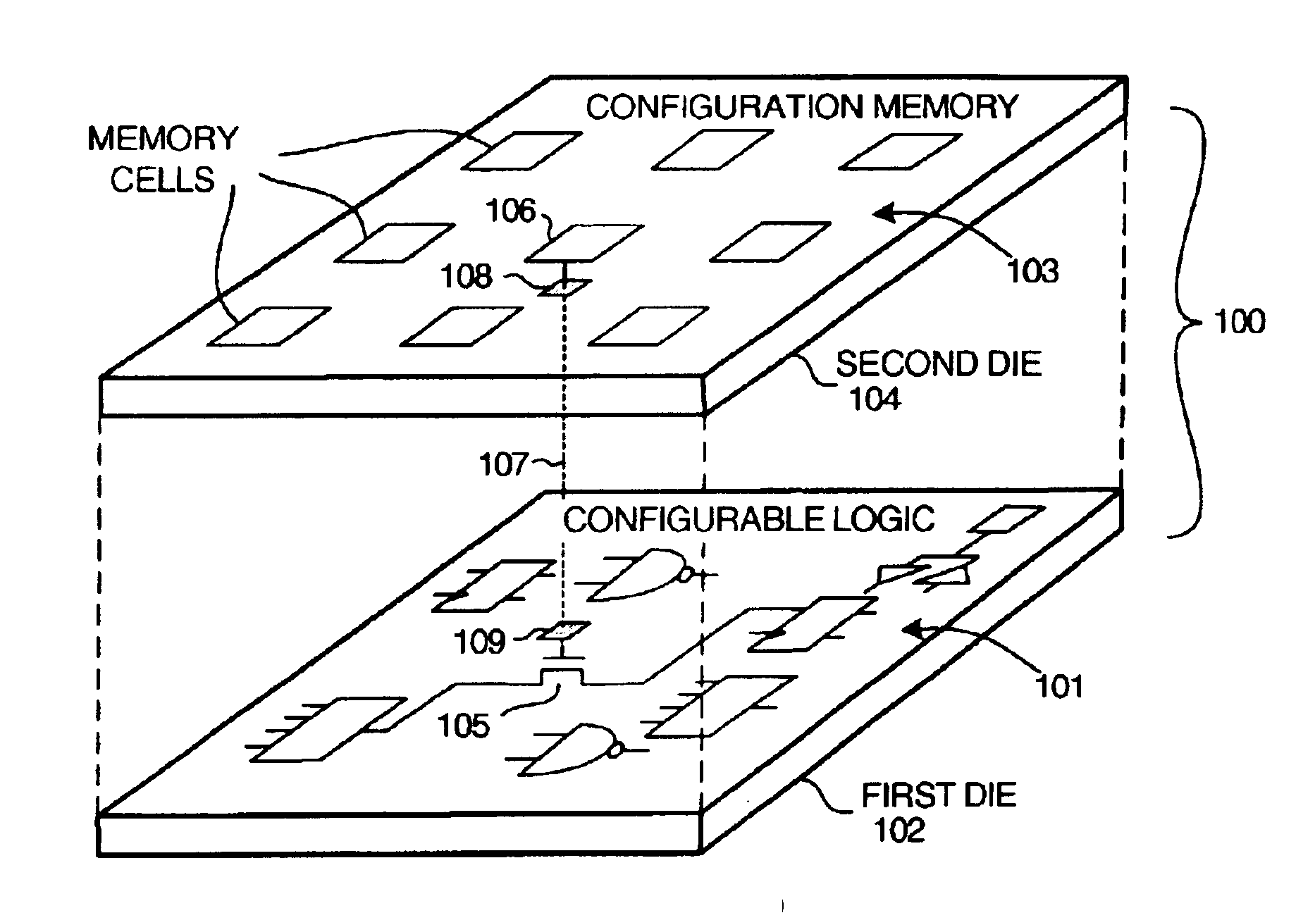
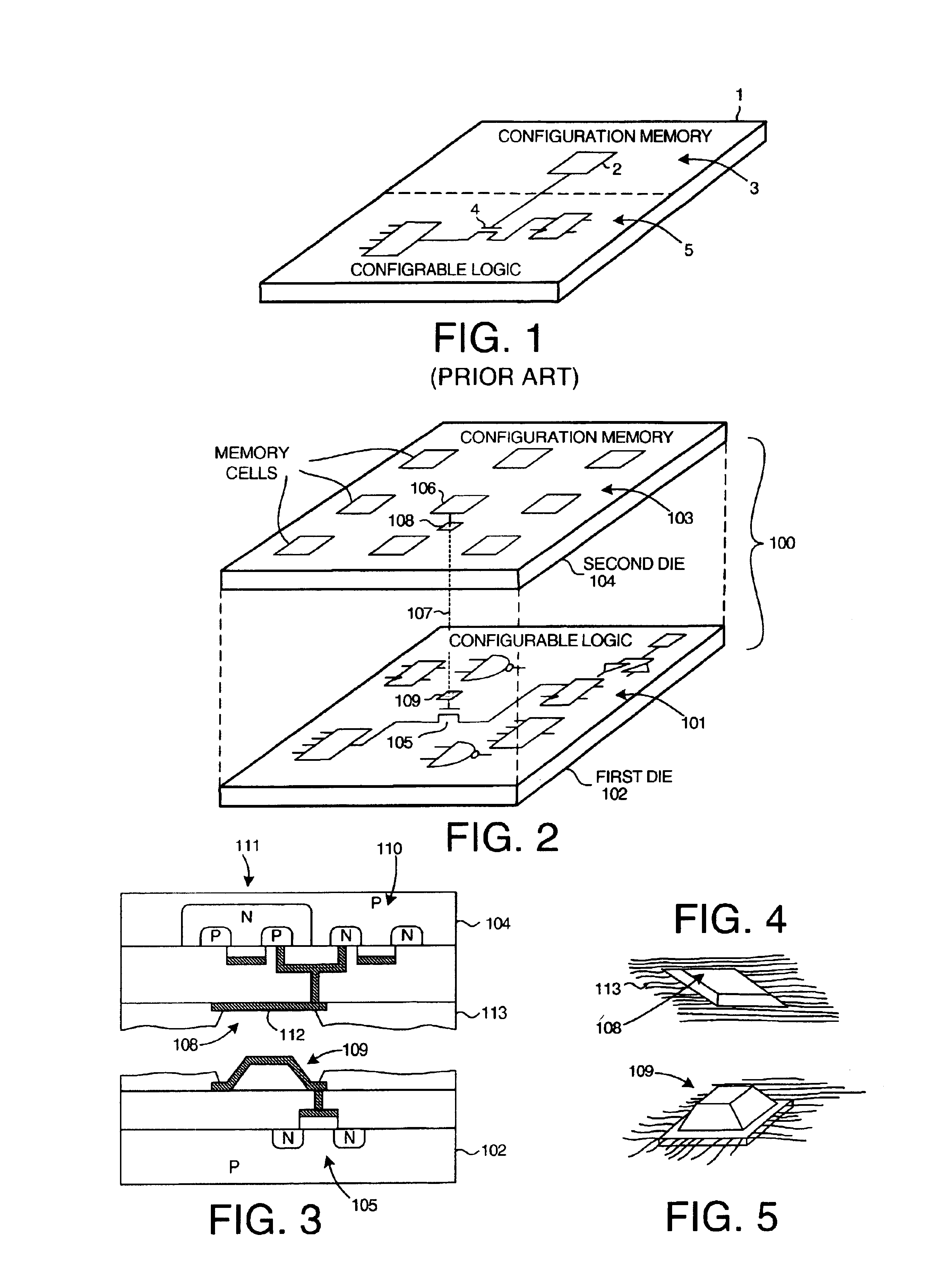
[0029]FIG. 2 is a simplified diagram of a programmable logic device in accordance with an embodiment of the present invention. In this example, the programmable logic device is a field programmable gate array (FPGA) 100. The circuitry of FPGA 100 is split such that all or substantially all of the configurable logic portion 101 of FPGA 100 is disposed on a first die 102, whereas all or substantially all of the configuration memory 103 of FPGA 100 is disposed on a second die 104. Second die 104 is coupled to first die 102 such that configuration data stored in configuration memory 103 is communicated to and configures the configurable logic portion 101. The configurable logic portion 101 so configured realizes a user-defined circuit.

[0030]In the example of FIG. 2, second die 104 is stacked on top of first die 102 in face-to-face relation such that the face side of first die 102 faces the face side of second die 104. The term face side used here denotes the side of the die that receive...


PUM


Abstract

The circuitry of a programmable logic device (for example, an FPGA) includes a configurable logic portion and a configuration memory. The configuration memory stores configuration data that configures the configurable logic portion to realize a user-defined circuit. The configurable logic portion is disposed on a first die whereas the configuration memory is disposed on a second die. The second die is bonded to the first die in stacked relation. Each bit of configuration data passes from the second die to the first die through a pair of micropads. One micropad of the pair is disposed on the first die and the other micropad of the pair is disposed on the second die. When the first die and second die are brought together in face-to-face relation, the two micropads form an electrical connection through which the configuration data bit passes from the second die to the first die.

Description

FIELD OF THE INVENTION[0001]The present invention relates to manufacturing of programmable logic devices.BACKGROUND OF THE INVENTION[0002]Programmable logic devices (PLDs), such as field-programmable gate arrays (FPGAs), are user-programmable integrated circuits that can be programmed to implement user-defined logic circuits. A typical FPGA architecture (for example, a Virtex FPGA available from Xilinx Inc. of San Jose Calif.), includes an array of configurable logic blocks (CLBs), a programmable interconnect structure, and programmable input / output blocks (IOBs). Each of the CLBs, the programmable interconnect structure, and the IOBs includes configuration memory cells, the contents of which determine how the CLB, the programmable interconnect structure, or the IOB is configured. To realize a user-defined circuit, configuration data is loaded into the configuration memory cells such that the CLBs and IOBs and programmable interconnect are configured to realize particular circuit co...

Claims


Application Information

Patent Timeline
IPC IPC(8): H01L25/065H01L25/18H01L27/02H01L27/118
CPCH01L24/11H01L24/81H01L25/0657H01L25/18H01L23/3171H01L24/13H01L24/16H01L25/50H01L27/0207H01L27/11803H01L27/11898H01L2224/114H01L2224/1147H01L2224/11616H01L2224/13082H01L2224/13099H01L2224/131H01L2224/13147H01L2224/1412H01L2224/16148H01L2224/81141H01L2224/81193H01L2224/81203H01L2224/81801H01L2224/81898H01L2224/819H01L2225/06513H01L2225/06527H01L2225/06541H01L2225/06593H01L2924/01013H01L2924/01029H01L2924/01073H01L2924/01006H01L2924/0102H01L2924/01023H01L2924/01033H01L2924/014H01L2924/14H01L2924/00
Inventor NEW, BERNARD J.
Owner XILINX INC
Why Eureka
Try Eureka