Space-saving packaging of electronic circuits

a technology of electronic circuits and packaging techniques, applied in the field of packaging techniques for electronic circuits, can solve the problems of limited space available for needed circuitry, limited use of valuable package volume, and inability to perform all the needed (or desired) functions of single integrated circuits, and achieve the effect of simplifying electrical connections

Inactive Publication Date: 2006-07-04
ALFRED E MANN FOUND FOR SCI RES
View PDF61 Cites 368 Cited by
  • Summary
  • Abstract
  • Description
  • Claims
  • Application Information

AI Technical Summary

Benefits of technology

[0003]The present invention is directed to a packaging technique for stacking a plurality of integrated circuit substrates which provides interconnection paths through the substrates to simplify electrical connections between the integrated circuits while facilitating minimization of the volume and customization of the ...

Problems solved by technology

Complex electronic devices typically require a large number of transistors, large enough that a single integrated circuit may not be able to perform all of the needed (or desired) functions.
With such lim...

Method used


Image

  • Space-saving packaging of electronic circuits
  • Space-saving packaging of electronic circuits
  • Space-saving packaging of electronic circuits

Examples


Embodiment Construction

[0018]The following description is of the best mode presently contemplated for carrying out the invention. This description is not to be taken in a limiting sense, but is made merely for the purpose of describing the general principles of the invention. The scope of the invention should be determined with reference to the claims.

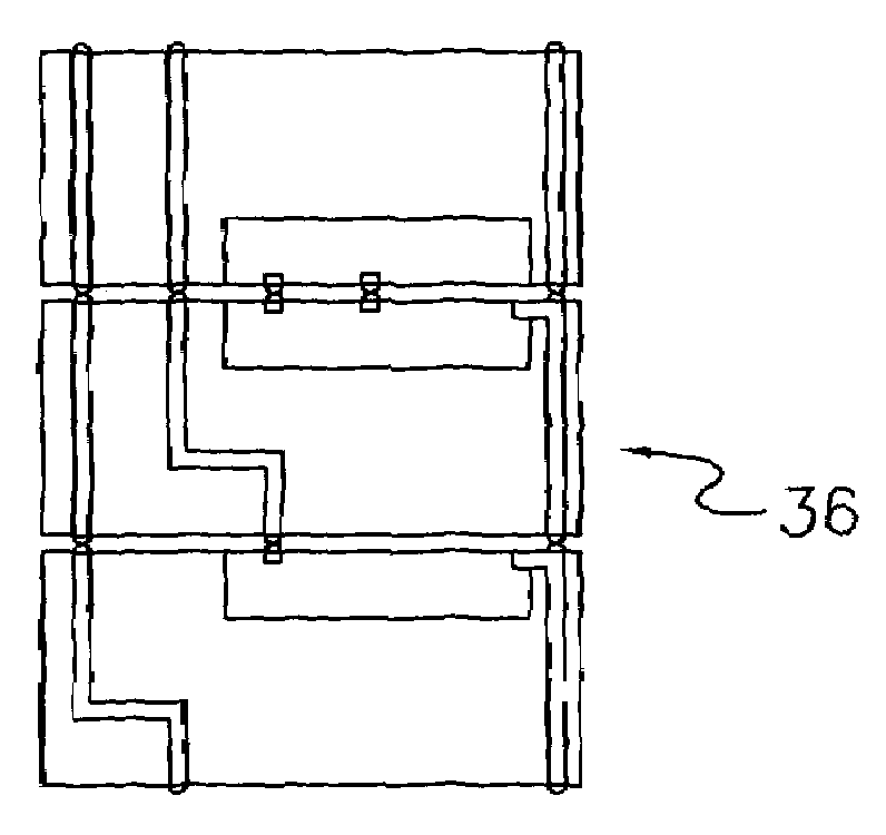
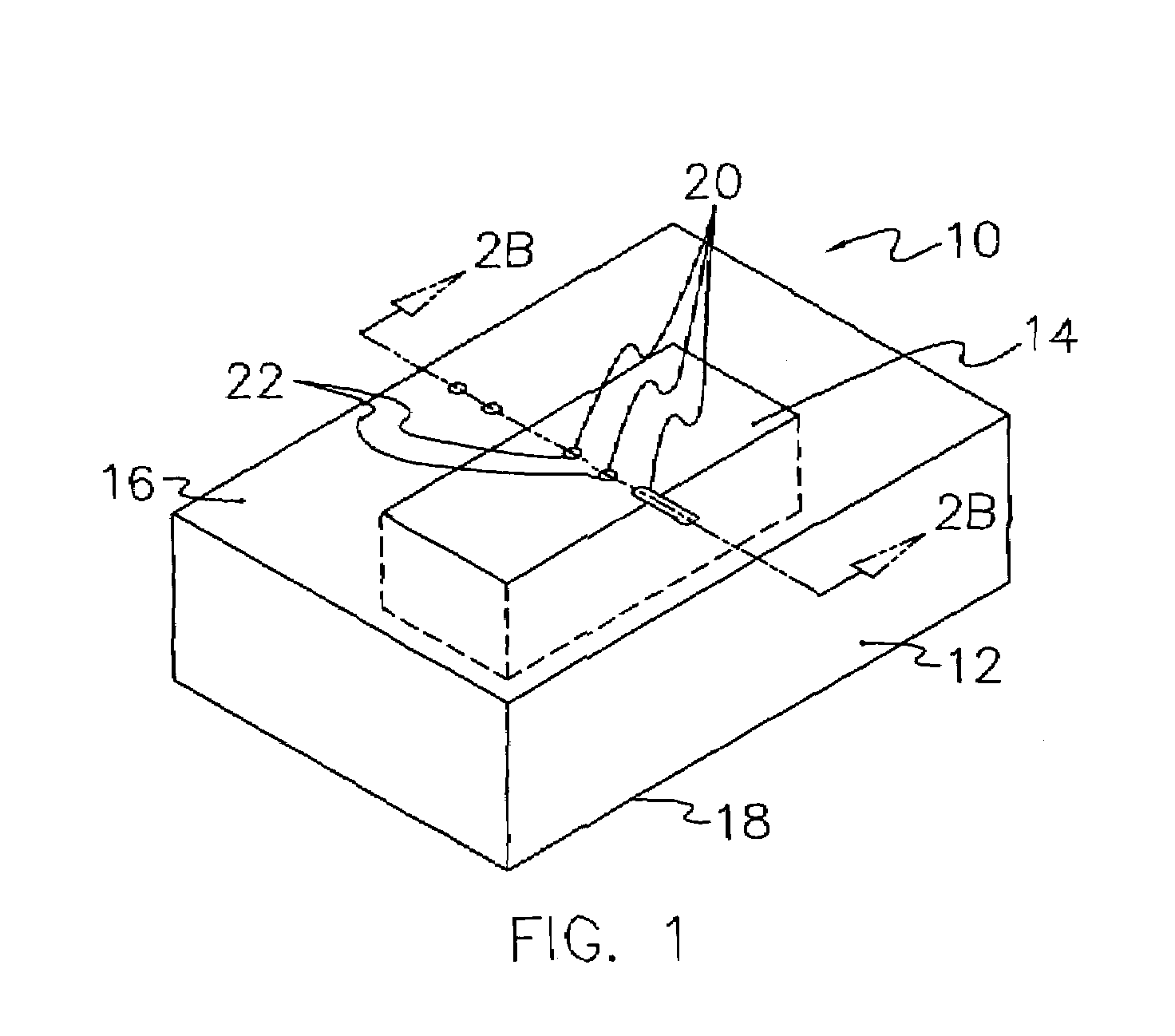
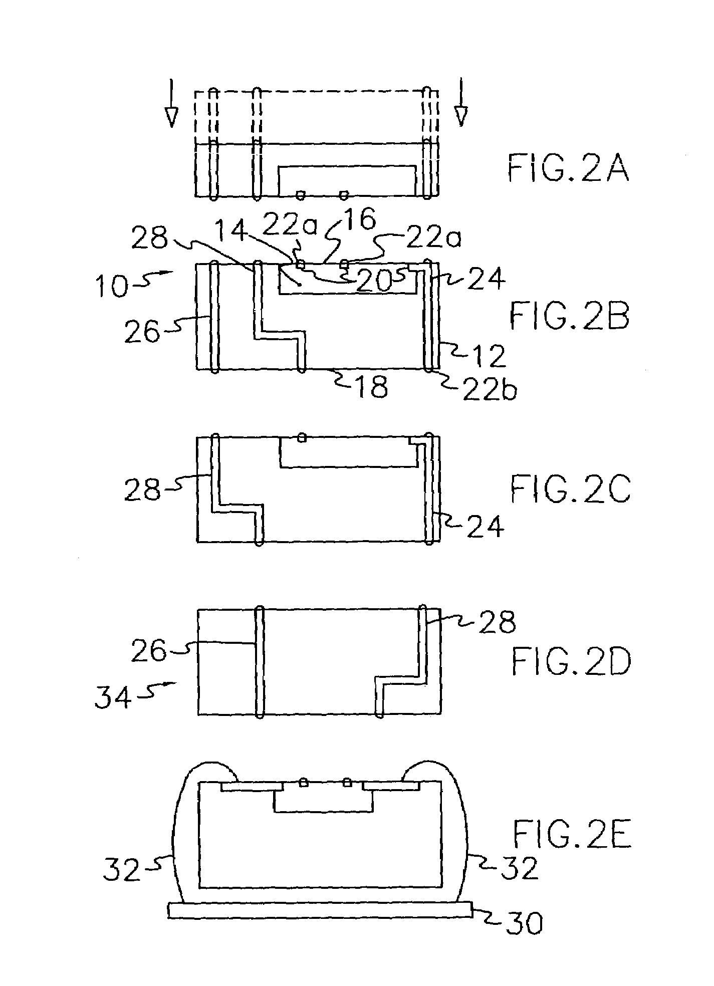
[0019]The present invention is directed to a packaging technique for stacking a plurality of integrated circuit substrates which provides interconnection paths through the substrates to simplify electrical connections between the integrated circuits while facilitating minimization of the volume and customization of the three dimensional package size to conform to the available internal space within a housing, e.g., one used in an implantable device where package volume is at a premium. Furthermore, an internal cavity can be created by the stacked formation that is suitable for mounting of a surface mount device, e.g., a crystal or the like. Advantageously, b...


PUM

PropertyMeasurementUnit
Lengthaaaaaaaaaa
Lengthaaaaaaaaaa
Electrical conductivityaaaaaaaaaa

Abstract

An apparatus and packaging method for stacking a plurality of integrated circuit substrates, i.e., substrates having integrated circuits formed as integral portions of the substrates, which provides interconnection paths through the substrates to simplify electrical connections between the integrated circuits while facilitating minimization of the volume and customization of the three dimensional package size to conform to the available internal space within a housing, e.g., one used in an implantabie device where package volume is at a premium. Furthermore, an internal cavity can be created by the stacked formation that is suitable for mounting of a surface mount device, e.g., a crystal or the like.

Description

FIELD OF THE INVENTION[0001]The present invention is generally directed to packaging techniques for electronic circuitry and in particular vertical stacking and interconnection techniques for a plurality of integrated circuits.BACKGROUND OF THE INVENTION[0002]Complex electronic devices typically require a large number of transistors, large enough that a single integrated circuit may not be able to perform all of the needed (or desired) functions. Accordingly, such devices are typically fabricated from a plurality of integrated circuit chips that are then interconnected via a motherboard or the like, e.g., a hybrid circuit. While the use of flip chips and BGAs (ball grid arrays) are known for simplifying interconnection between the chips (along with wire bonds), such interconnection techniques can use up valuable and sometimes limited internal package volume. For example, U.S. Pat. Nos. 6,164,284; 6,185,452; 6,208,894; 6,315,721; and 6,472,991; and copending, commonly-assigned U.S. p...

Claims


Application Information

Patent Timeline
IPC IPC(8): H01L23/02H01L25/065
CPCH01L23/481H01L25/0657H01L2225/06513H01L2225/0652H01L2225/06541H01L2224/16146Y10T29/53104H01L2224/131H01L2224/13025H01L2224/14181H01L2225/06572H01L2924/014H01L2224/05571H01L2224/05573
Inventor FEY, KATE E.BYERS, CHARLES L.MANDELL, LEE J.
Owner ALFRED E MANN FOUND FOR SCI RES
Why Eureka
Try Eureka