Method of processing a substrate

a substrate and processing technology, applied in the direction of semiconductor/solid-state device details, separation processes, instruments, etc., can solve the problems of difficult scaling up to treat objects larger than about a square foot, ion-induced damage of the substrate, and low concentration of reactive species to achieve the desired etching or deposition ra

Inactive Publication Date: 2008-02-12
RGT UNIV OF CALIFORNIA
View PDF48 Cites 175 Cited by
  • Summary
  • Abstract
  • Description
  • Claims
  • Application Information

AI Technical Summary

Problems solved by technology

In most applications, the ions are kept away from the chemical precursors as much as possible, because the ions may cause non-selective decomposition with the incorporation of unwanted impurities into the CVD film.
However, in this case, ion-induced damage of the substrate may occur.
A disadvantage of plasmas operating at low pressures is that the concentration of reactive species can be too low to give the desired etching or deposition rate.
Another disadvantage of low-pressure plasmas is that they are difficult to scale up to treat objects that are larger than about a square foot in area.
Therefore, designing a plasma reactor requires many hours of engineering and experimentation, all of which greatly adds to the cost of the device.
A further disadvantage of low-pressure plasmas is that the reactive gas fills the entire volume inside the vacuum chamber.
In these devices, it is impossible to completely separate the ions from the neutral reactive species.
Ions always impinge on the substrate, and may cause damage, if, for example, it contains sensitive electronic devices, such as solid-state transistors.
The ions and reactive gases may also damage the chamber and other system components, including the substrate holder, the gas injection rings, the electrodes, and any quartz dielectric parts.
These deposits alter the characteristics of the plasma as well as lead to particulate contamination problems.
However, the residues are of different thickness and their rates of etching may not be uniform, making it difficult to satisfactorily clean all the surfaces.
These cleaning operations add to the cost of operating the plasma device and are a significant disadvantage.
While these devices can provide high concentrations of reactants for etching and deposition, they have other disadvantages that make them unsuitable for many materials applications.
This device may be used for processing materials at high temperatures, such as in metal welding, but is not useful for etching and depositing thin films as described in the preceding paragraphs.
A drawback of these devices is that the plasmas are not uniform throughout the space between the electrodes.
In addition, they do not produce the same reactive chemical species as are present in low-pressure plasmas of similar gas composition.
These designs have a serious drawback in that they do not treat large areas uniformly.
Scaling them up to cover larger areas, such as a square foot of material, is not straightforward and may not be possible.

Method used


Image

  • Method of processing a substrate
  • Method of processing a substrate
  • Method of processing a substrate

Examples


Embodiment Construction

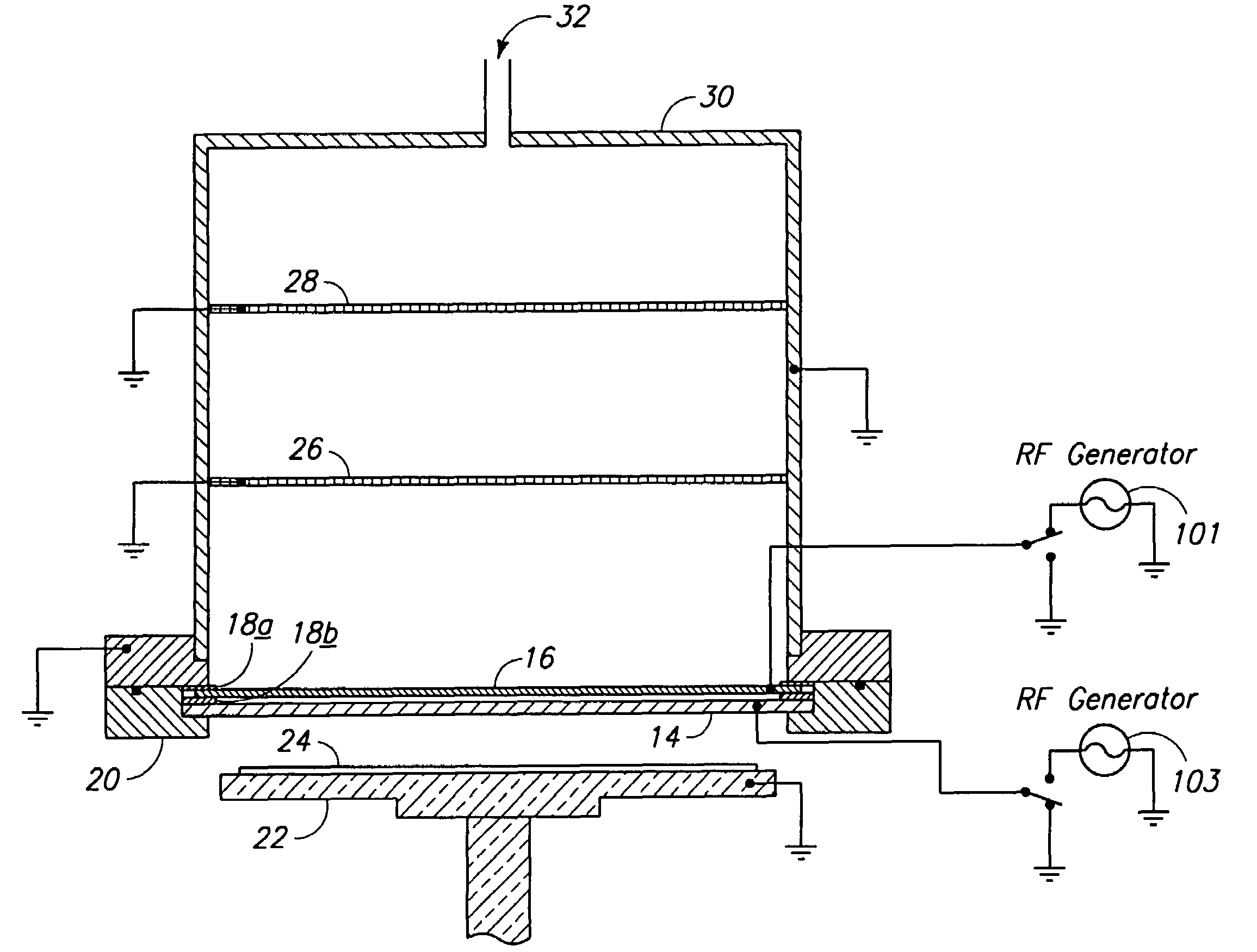
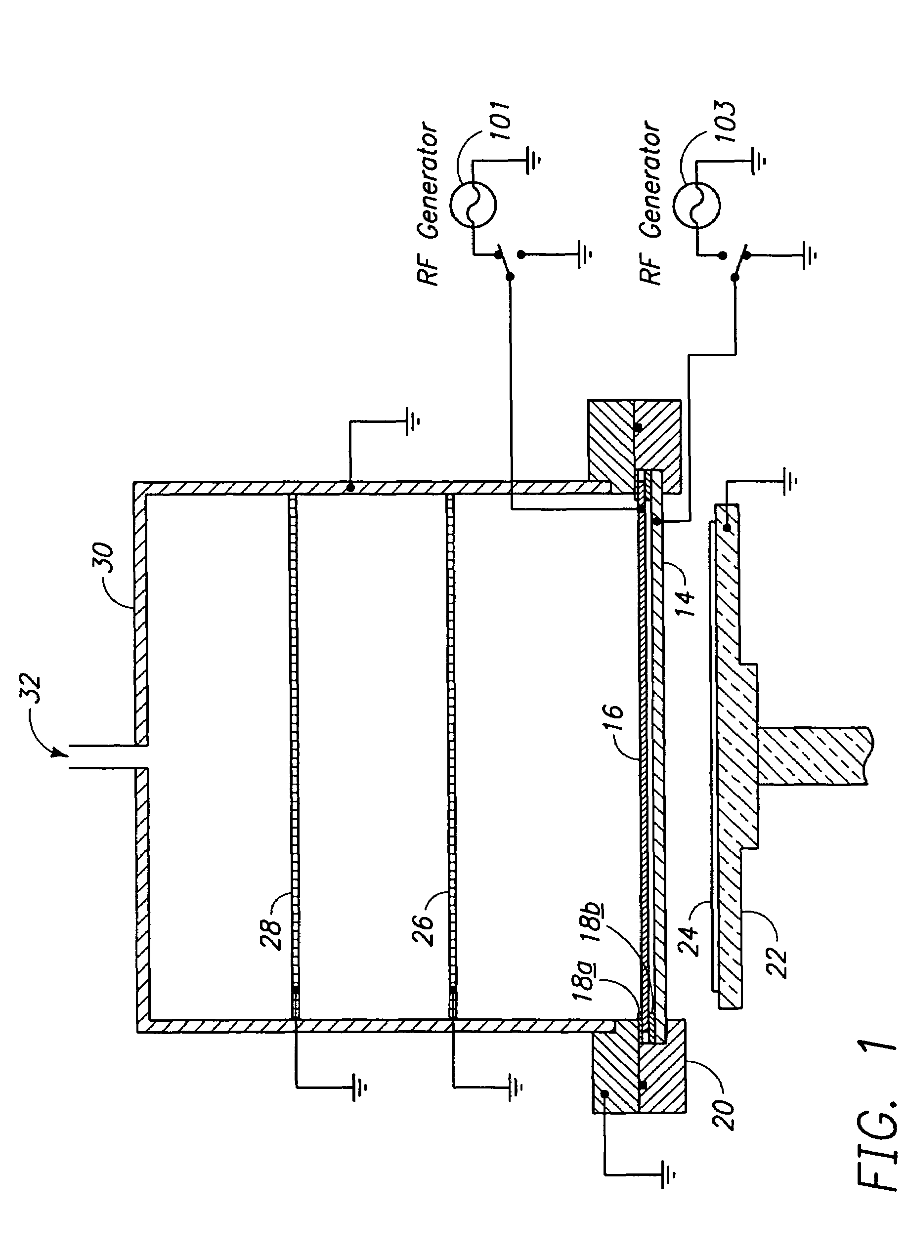
[0037]In the following description of the preferred embodiment, reference is made to the accompanying drawings which form a part hereof, and in which is shown by way of illustration the specific embodiment in which the invention may be practiced. It is to be understood that other embodiments may be utilized and structural and functional changes may be made without departing from the scope of the present invention.

Overview

[0038]The invention is embodied in a plasma flow device or reactor having a housing that contains conductive electrodes with openings to allow gas to flow through or around them, where one or more of the electrodes are powered by an RF source and one or more are grounded, and a substrate or work piece is placed in the gas flow downstream of the electrodes, such that said substrate or work piece is substantially uniformly contacted with the reactive gases emanating therefrom over a large surface area of the substrate. The invention is also embodied in a plasma flow d...


PUM

PropertyMeasurementUnit
temperatureaaaaaaaaaa
pressuresaaaaaaaaaa
temperatureaaaaaaaaaa

Abstract

The invention is embodied in a plasma flow device or reactor having a housing that contains conductive electrodes with openings to allow gas to flow through or around them, where one or more of the electrodes are powered by an RF source and one or more are grounded, and a substrate or work piece is placed in the gas flow downstream of the electrodes, such that said substrate or work piece is substantially uniformly contacted across a large surface area with the reactive gases emanating therefrom. The invention is also embodied in a plasma flow device or reactor having a housing that contains conductive electrodes with openings to allow gas to flow through or around them, where one or more of the electrodes are powered by an RF source and one or more are grounded, and one of the grounded electrodes contains a means of mixing in other chemical precursors to combine with the plasma stream, and a substrate or work piece placed in the gas flow downstream of the electrodes, such that said substrate or work piece is contacted by the reactive gases emanating therefrom. In one embodiment, the plasma flow device removes organic materials from a substrate or work piece, and is a stripping or cleaning device. In another embodiment, the plasma flow device kills biological microorganisms on a substrate or work piece, and is a sterilization device. In another embodiment, the plasma flow device activates the surface of a substrate or work piece, and is a surface activation device. In another embodiment, the plasma flow device etches materials from a substrate or work piece, and is a plasma etcher. In another embodiment, the plasma flow device deposits thin films onto a substrate or work piece, and is a plasma-enhanced chemical vapor deposition device or reactor.

Description

CROSS-REFERENCE TO RELATED APPLICATIONS[0001]This application claims priority under 35 U.S.C. § 119(e) of U.S. Provisional Patent Application No. 60 / 134,353, filed May 14, 1999, entitled “PLASMA FLOW DEVICE,” by Steven E. Babayan et al., which application is incorporated by reference herein.[0002]This application is a continuation of application Ser. No. 09 / 567,851, filed May 9, 2000, by Steven B. Babayan and Robert F. Hicks, entitled “LOW-TEMPERATURE COMPATIBLE WIDE-PRESSURE-RANGE PLASMA FLOW DEVICE”, which claims the benefit of provisional Application Ser. No. 60 / 134,353, filed May 14, 1999 by Steven E. Babayan and Robert F. Hicks, entitled “PLASMA FLOW DEVICE”.STATEMENT REGARDING FEDERALLY SPONSORED RESEARCH OR DEVELOPMENT[0003]This invention was made with Government support under Grant No. DE-F5607-96ER-45621, awarded by the U.S. Department of Energy, Basic Energy Sciences. The Government has certain rights in this invention.BACKGROUND OF THE INVENTION[0004]1. Field of the Inven...

Claims


Application Information

Patent Timeline
Patent Type & Authority Patents(United States)
IPC IPC(8): H01L21/3065B01D53/26G01N27/12G02F1/13H01L23/08H01L23/10H01L23/26H01L51/52H01L51/56
CPCH01L23/08H01L23/10H01L23/26H01L51/524H01L51/5246H01L2924/0002H01L2251/566H01L2924/01079H01L2924/09701H01L2924/12044H01L2924/16152H01L2924/16195H01L2924/3011H01L51/5253H01L51/5259H01L2924/00H10K50/846H10K50/8426H10K50/844H10K71/851G02F1/13H10K50/841
Inventor BABAYAN, STEVEN E.HICKS, ROBERT F.
Owner RGT UNIV OF CALIFORNIA
Why Eureka
Try Eureka