Apparatus and method for depositing low K dielectric materials

Inactive Publication Date: 2001-01-23
APPLIED MATERIALS INC
View PDF8 Cites 271 Cited by
  • Summary
  • Abstract
  • Description
  • Claims
  • Application Information

AI Technical Summary

Problems solved by technology

These required changes are costly and do not pr

Method used


Image

  • Apparatus and method for depositing low K dielectric materials
  • Apparatus and method for depositing low K dielectric materials
  • Apparatus and method for depositing low K dielectric materials

Examples


Embodiment Construction

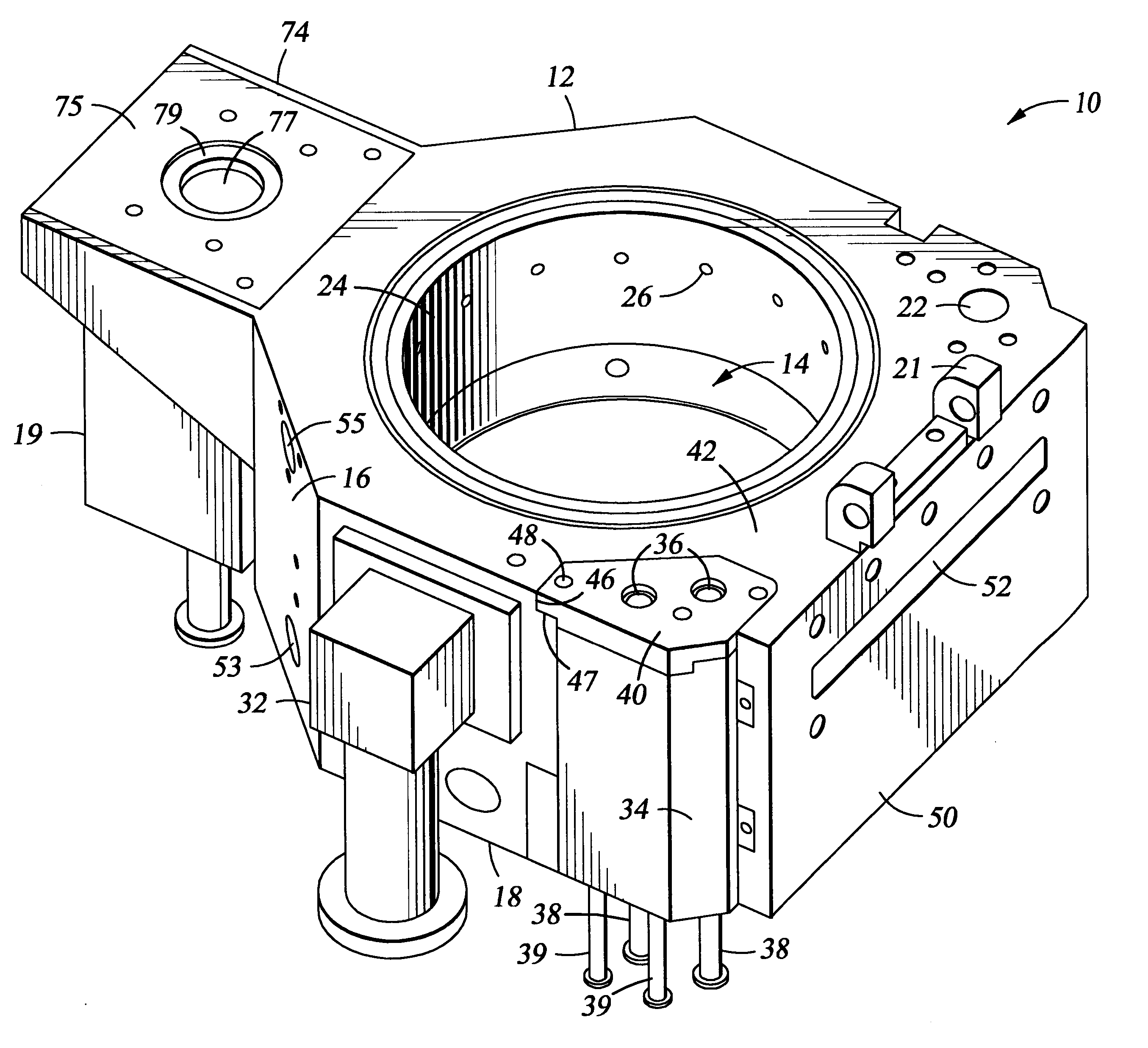
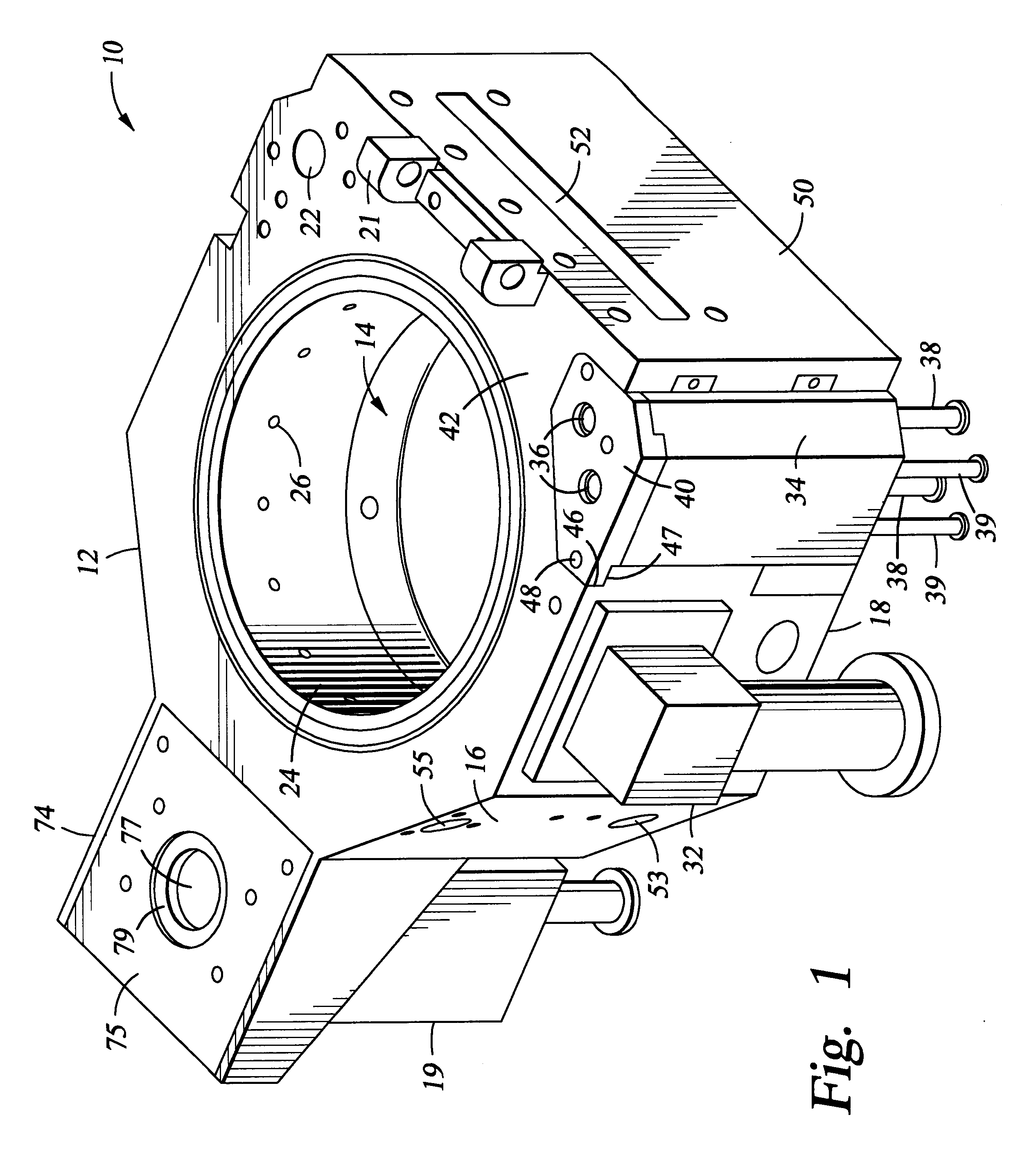
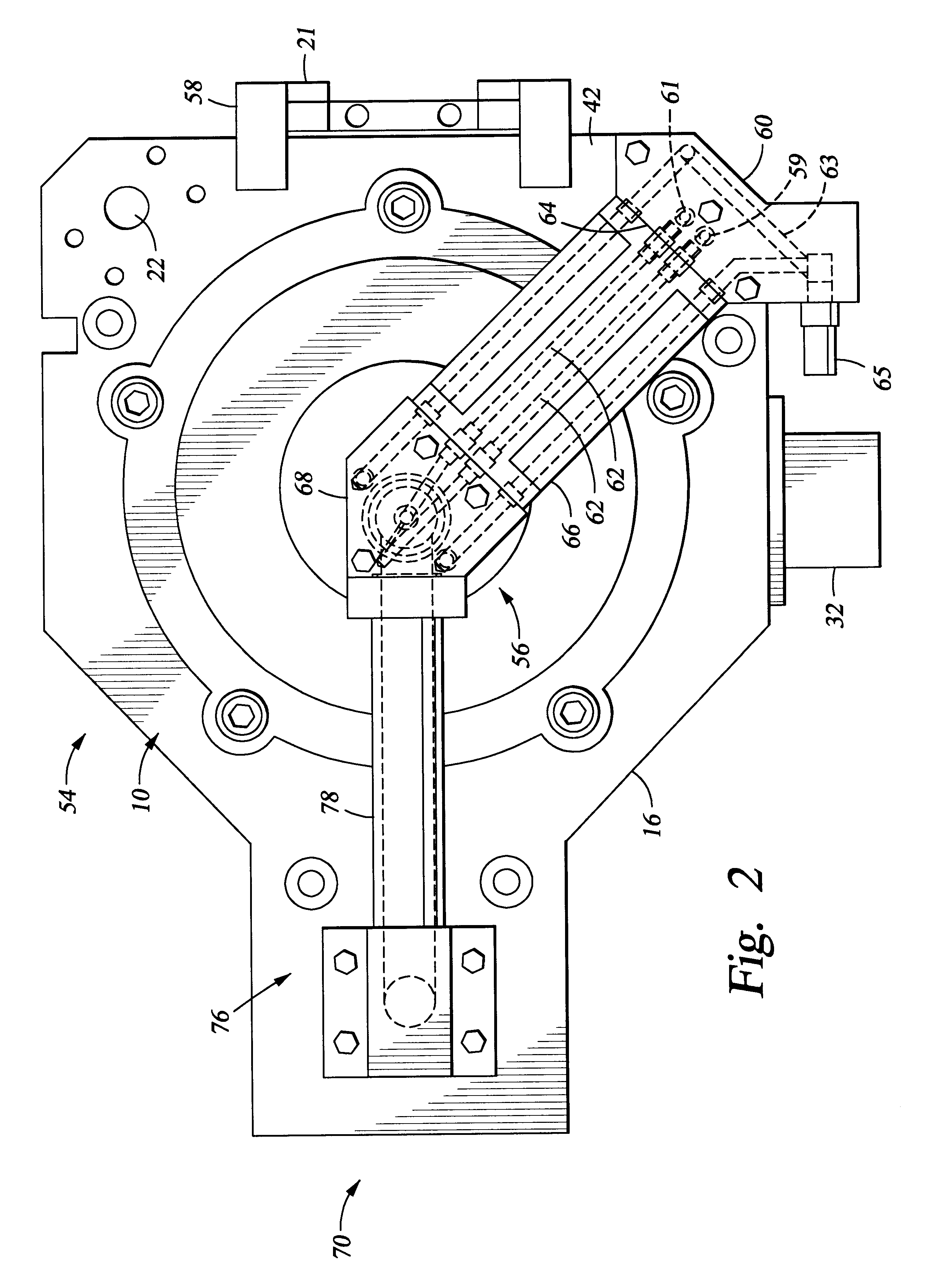
FIG. 1 is a substantially top perspective view showing one embodiment of a chamber 10 of the present invention. Generally, the chamber 10 includes a chamber body 12 defining a central processing region 14. The chamber body includes a sidewall 16 and a bottom 18 which is preferably made of stainless steel or aluminum. In the embodiment shown, the processing region is a cylindrical region defined in the chamber body. However, the processing region can be configured in other shapes and sizes to accommodate the shape and size of the substrate being processed. A nose 74 of the chamber preferable supports a microwave applicator 19 wherein cleaning gases and other process gases can be excited using microwave energy and delivered into the gas distribution system. A lid (shown in FIG. 2) is hingedly mounted on the upper portion of the process chamber at hinge 21 and includes the gas distribution assembly (also shown in FIG. 2) disposed thereon.

The chamber body 12 defines an electrical feedth...


PUM

PropertyMeasurementUnit
Dielectric polarization enthalpyaaaaaaaaaa

Abstract

The invention provides a deposition system and methods of depositing materials onto substrates. In one aspect, a modular processing chamber is provided which includes a chamber body defining a processing region. The chamber body includes a removable gas feedthrough, an electrical feedthrough, a gas distribution assembly mounted on a chamber lid and a microwave applicator for generating reactive gases remote from the processing region.

Description

1. Field of the InventionThe present invention relates to a processing system and more particularly to a chemical vapor deposition chamber useful for depositing dielectric materials on substrates during the fabrication of integrated circuits and other electronic devices.2. Background of the Related ArtIn the fabrication of integrated circuits and other electronic devices on substrates, multiple deposition and etch steps are performed in sequence to fabricate the desired electronic structures or devices. The trend has been to reduce the overall size of the features which make up the devices and to increase the density of devices formed on a single die. The goal in designing and fabricating these electronic devices is to achieve an overall increase in the speed and capacity of the overall device. This trend has caused a significant amount of research to be undertaken in the area of materials to accomplish these goals. As dimensions decrease, a need arises for materials with lower diel...

Claims


Application Information

Patent Timeline
IPC IPC(8): C23C16/44C23C16/455C23C16/448C23C16/452H01J37/32
CPCC23C16/4405C23C16/452C23C16/455H01J37/32192H01J37/32458
Inventor KAO, YEH-JENCHANG, FONG M.MAJEWSKI, ROBERT B.PARKS, JOHNWANAMAKER, DAVIDWANG, YEN-KUN
Owner APPLIED MATERIALS INC
Why Eureka
Try Eureka