Dielectric passivation for semiconductor devices

a technology of semiconductor devices and passivation layers, applied in semiconductor devices, semiconductor/solid-state device details, electrical apparatus, etc., can solve problems such as the drawback of possibly interfering with the operation of the device, affecting the performance of the device in undesirable ways, and limited to protecting the device from outside elements

Active Publication Date: 2008-02-19
CREE INC
View PDF21 Cites 95 Cited by
  • Summary
  • Abstract
  • Description
  • Claims
  • Application Information

AI Technical Summary

Benefits of technology

[0017]In another aspect the invention is a semiconductor device comprising a layer of Group III nitride semiconductor material that includes at least one surface, a control contact on said surface for controlling the electrical response of said semiconductor material, a silicon dioxide barrier layer covering at least a portion of said one surface adjacent said control contact, for providing a bandgap greater than the bandgap of said Group III nitride and a conduction band offset from the conduction band of said Group III nitride, and a silicon nitride protective layer covering the remainder of said Group III nitride surface for providing a physical and chemical barrier against moisture, oxygen and related environmental attack.
[0018]In another aspect the invention is a semiconductor device comprising a layer of Group III nitride semiconductor material that includes at least one surface, a control contact on said surface for controlling the electrical response of said semiconductor material, a silicon dioxide barrier layer covering at least a portion of said one surface adjacent said control contact, said dielectric barrier layer having a bandgap greater than the bandgap of said Group III nitride and a conduction band offset from the conduction band of said Group III nitride, a silicon nitride protective layer covering the remainder of said Group III nitride surface for providing a physical and chemical barrier against moisture, oxygen and related environmental attack, and a spacer layer interposed between said Group III nitride surface and said silicon dioxide barrier layer for physically protecting said Group III nitride surface and for reducing surface charge accumulation.

Problems solved by technology

The accumulation of charge carriers within energy states along the surface of the device and within the passivation layers themselves affects device performance in undesirable ways.
Passivation layers, however, have the drawback of possibly interfering with the operation of the device.
The Nariani patent, however, is limited to protecting the device from outside elements and provides no additional control over the electro-chemical processes at work within the device itself.
Protecting an overall device from outside elements is a worthy endeavor, but encapsulating a device with a passivation layer may not necessarily protect the device from undesired internal chemical or electrical interactions that can affect the electrical response within the device.
Simple encapsulation of certain devices with an oxide or nitride layer may be ineffective to provide sufficient environmental protection, device stability, and simultaneous optimization of performance.
A small input signal applied to the gate may modulate a relatively large amount of current in the channel, resulting in signal amplification if an appropriate load is presented.
If the control contact is a contact directly on the surface of the semiconductor, other mobile or trapped charges on or near the surfaces adjacent to the control contact of such devices can hinder proper modulation of the conductive channel by the control voltage.
A recurring problem in achieving the proper control bias is the presence of energy states at or near the intersection of the control contact and the semiconductor body.
The charged states significantly deteriorate performance of semiconductor devices by affecting the current flow in the conducting layer below the areas adjacent to the gate.
Charge carriers trapped within these energy states are problematic, as they affect the overall electrical characteristics of the device.
For example, since electric charges give rise to electric fields, accumulated charge carriers may cause unwanted electric fields to be present in the semiconductor structure.

Method used


Image

  • Dielectric passivation for semiconductor devices
  • Dielectric passivation for semiconductor devices
  • Dielectric passivation for semiconductor devices

Examples


first embodiment

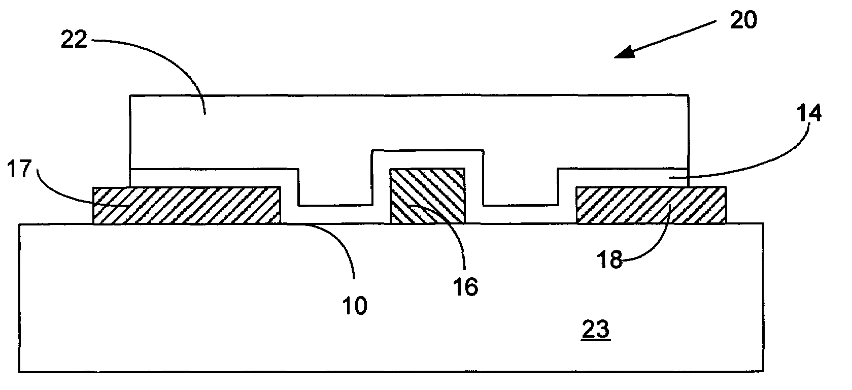
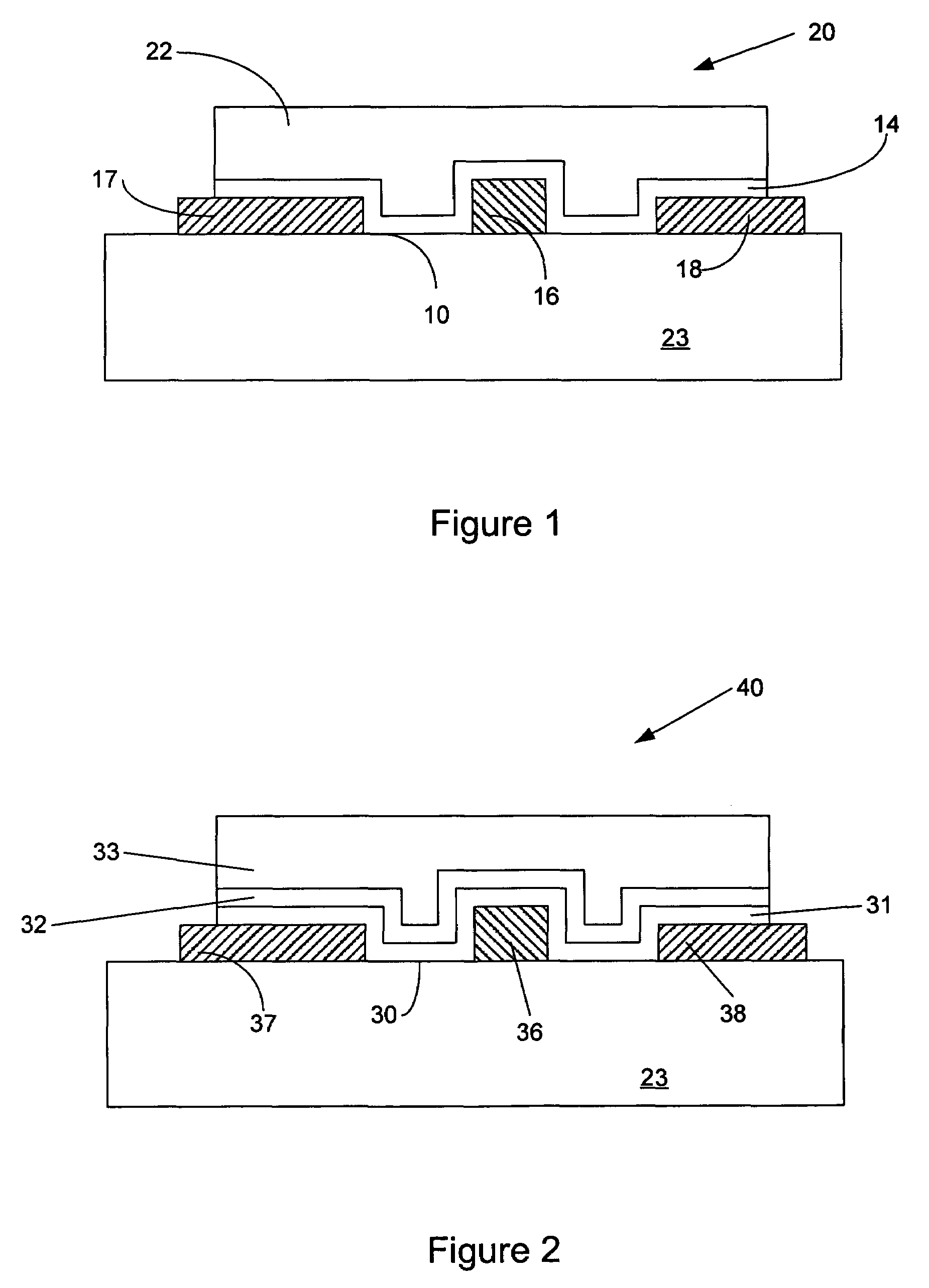
[0032]the invention is illustrated in FIG. 1 and includes a semiconductor device precursor structure 20 based upon a Group III nitride portion (substrate or epilayer) 23. The semiconductor device precursor 20 has at least one electrical contact 16 on its surface 10 with one of the electrical contacts essentially controlling the electrical behavior of the underlying Group III nitride material. For this specification, the inventors refer to this primary contact 16 as the control or gate contact. This terminology is for convenience of discussion only and is not intended to limit the nature of the invention herein. The electrical response of the semiconductor includes, but is not limited to, overall current flow, carrier flow and recombination, voltage response, and any other electrical variations within the semiconductor that are well known in the art of semiconductor electronics.

[0033]In addition to a gate contact 16, the structure 20 illustrated in FIG. 1 includes a source contact 18...

embodiment 21

[0035]FIG. 6 illustrates an embodiment 21 analogous to FIG. 1, but in which the charge barrier layer 14 covers a portion, but not all, of the surface 10 adjacent the gate contact 16 extending toward the source contact 18, and in which the charge barrier layer 14 also covers a portion, but not all, of the surface 10 adjacent the gate contact 16 extending toward the drain contact 17. The charge barrier layer 14 should be present in areas in which there are large electric fields which are capable of imparting sufficient energy to carriers to enable them to surmount the energy barrier presented by the protective layer 22. Accordingly, it may be particularly important for the charge barrier layer 14 to extend along the drain-side edge of the gate 16. In some embodiments, the charge barrier layer 14 may extend along the drain-side edge of the gate contact 16 for a distance of between about 0.25 and 5 microns. The charge barrier layer 14 may extend along the source-side edge of the gate co...

second embodiment

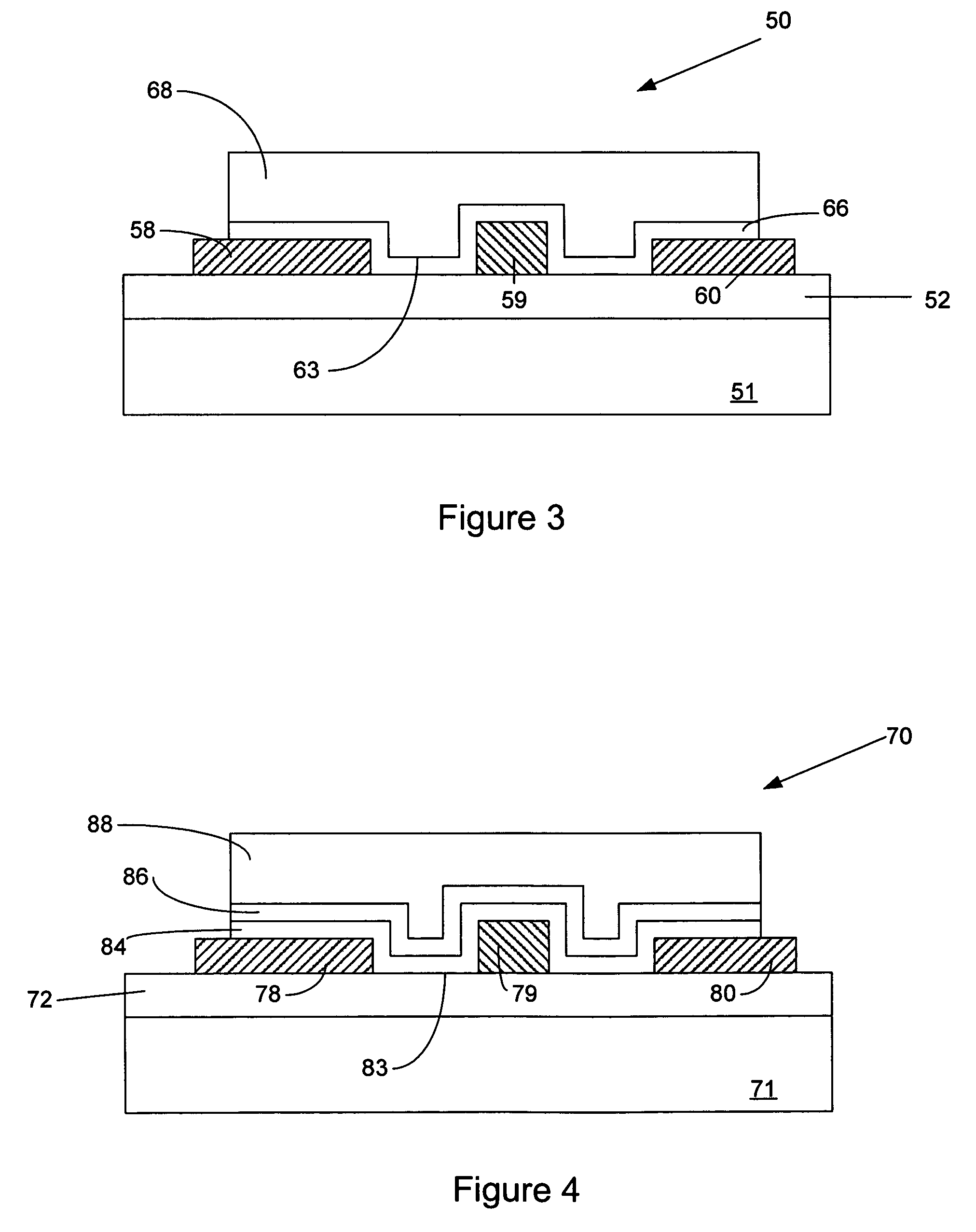
[0071]As in the second embodiment, the spacer layer 84 may be extremely thin and still provide a protective coating to the semiconductor surface in accordance with the invention herein. The charge barrier layer 86 and the protective layer 88 may, therefore, be thicker than the spacer layer 84. The protective layer 88 is typically much thicker than the charge barrier layer 86. The layers are shown schematically in FIG. 4, and actual devices would have the relative thicknesses described above. The charge barrier layer 86 may be between about 5 and 200 nanometers in thickness. In some embodiments, the charge barrier layer 86 is about 100 nanometers thick. The spacer layer 84 may be between about 0.5 and about 5 nanometers thick.

[0072]The spacer layer 84, charge barrier layer 86, and protective layer 88 of the fourth embodiment are identical to that of the third embodiment. The SiO2 charge barrier layer 86 is deposited by a method selected from the group consisting of plasma-enhanced ch...


PUM


Abstract

A semiconductor device is disclosed that includes a layer of Group III nitride semiconductor material that includes at least one surface, a control contact on the surface for controlling the electrical response of the semiconductor material, a dielectric barrier layer covering at least a portion of the one surface adjacent the control contact, the dielectric barrier layer having a bandgap greater than the bandgap of the Group III nitride and a conduction band offset from the conduction band of the Group III nitride; and a dielectric protective layer covering the remainder of the Group III nitride surface.

Description

BACKGROUND OF THE INVENTION[0001]The invention relates to passivation layers that protect semiconductor devices from hostile environmental conditions and help control electrical properties of the outer semiconductor layers of the devices. In particular, the invention pertains to protective layers of dielectric materials with appropriate physical properties to provide means for improving the surface quality and electrical performance of a semiconductor device.[0002]The accumulation of charge carriers within energy states along the surface of the device and within the passivation layers themselves affects device performance in undesirable ways. Passivation layers are known to provide a dual benefit of helping to protect semiconductor surfaces against environmental contamination while also reducing the density of interface traps present at the surface of the material at which charge can accumulate.[0003]Passivation layers, however, have the drawback of possibly interfering with the ope...

Claims


Application Information

Patent Timeline
Patent Type & Authority Patents(United States)
IPC IPC(8): H01L23/58H01L21/31H01L21/314H01L21/316H01L21/335H01L23/31H01L29/20H01L29/778H01L31/108
CPCH01L29/66462H01L29/7787H01L31/1085H01L23/3192H01L29/2003H01L2924/0002H01L2924/00H01L21/0214H01L21/02164H01L21/0217H01L21/022H01L21/02266H01L21/02271H01L21/02274
Inventor SMITH, RICHARD PETERSHEPPARD, SCOTT T.PALMOUR, JOHN WILLIAMS
Owner CREE INC
Why Eureka
Try Eureka