High frequency amplification circuit and mobile communication terminal using the same

a technology of high frequency amplification and mobile communication, applied in the direction of amplifiers with field-effect devices, amplification control device circuits, gain control, etc., can solve the problems of increasing control parameters and complicating the control circuit, so as to prevent the control circuit from being enlarged or complicated, and reduce the influence of gain

Inactive Publication Date: 2008-03-04
COLLABO INNOVATIONS INC
View PDF16 Cites 11 Cited by
  • Summary
  • Abstract
  • Description
  • Claims
  • Application Information

AI Technical Summary

Benefits of technology

[0019]Therefore, an object of the present invention is to provide a high frequency amplification circuit having a reduced influence on the gain exerted by a variation in the threshold voltage of the FET which is caused by, for example, inconsistencies in the production process or the operating temperature change, a high frequency amplification circuit having a broadened gain control range while preventing the control circuit from being enlarged or being complicated, and a mobile communication terminal using such a high frequency amplification circuit.
[0028]Alternatively, a high frequency amplification circuit according to the present invention comprises a terminal group including first and second signal input terminals to which first and second high frequency signals to be amplified are respectively to be input, first and second signal output terminals respectively for outputting the amplified high frequency signals, a gain control terminal to which a control voltage is to be applied, and a reference voltage terminal to which a reference voltage is to be applied; a first amplifier provided between the first signal input terminal and the first signal output terminal for amplifying the input first high frequency signal; a second amplifier provided between the second signal input terminal and the second signal output terminal for amplifying the input second high frequency signal; a first gain control circuit, provided between the first signal input terminal and the first signal output terminal and connected in series to the first amplifier, for changing an attenuation of the input first high frequency signal in accordance with the control voltage applied to the gain control terminal; a second gain control circuit, provided between the second signal input terminal and the second signal output terminal and connected in series to the second amplifier, for changing an attenuation of the input second high frequency signal in accordance with the control voltage applied to the gain control terminal; and a reference voltage circuit for generating first and second internal reference voltages from the reference voltage applied to the reference voltage terminal and supplying the generated first and second internal reference voltages respectively to the first and second gain control circuits. The first gain control circuit may include a first field effect transistor for receiving the control voltage at a gate terminal thereof, the first gain control circuit having a resistance value which is changed in accordance with the given control voltage. The second gain control circuit may include a second field effect transistor for receiving the control voltage at a gate terminal thereof, the second gain control circuit having a resistance value which is changed in accordance with the given control voltage. The reference voltage circuit may include a plurality of third field effect transistors for generating a voltage which is shifted with respect to the reference voltage by a threshold voltage of the third field effect transistors, and a voltage division circuit for dividing the generated voltage and generating the first and second internal reference voltages. The first and second gain control circuits may continuously change the attenuation of the input first and second high frequency signals respectively by the resistance values of the first and second field effect transistors being continuously changed. The reference voltage circuit may supply the first and second internal reference voltages generated by the voltage division circuit to source terminals and / or drain terminals of the first and second field effect transistors respectively, thereby counteracting influences exerted by the threshold voltages of the first and second field effect transistors on changes in the attenuation of the high frequency signals in the first and second gain control circuits, respectively.

Problems solved by technology

However, the above-described conventional gain control circuit has the following problems.
This enlarges the circuit scale of the D / A converter and thus increases the control parameters of the attenuation, which complicate the control circuit.

Method used


Image

  • High frequency amplification circuit and mobile communication terminal using the same
  • High frequency amplification circuit and mobile communication terminal using the same
  • High frequency amplification circuit and mobile communication terminal using the same

Examples


first embodiment

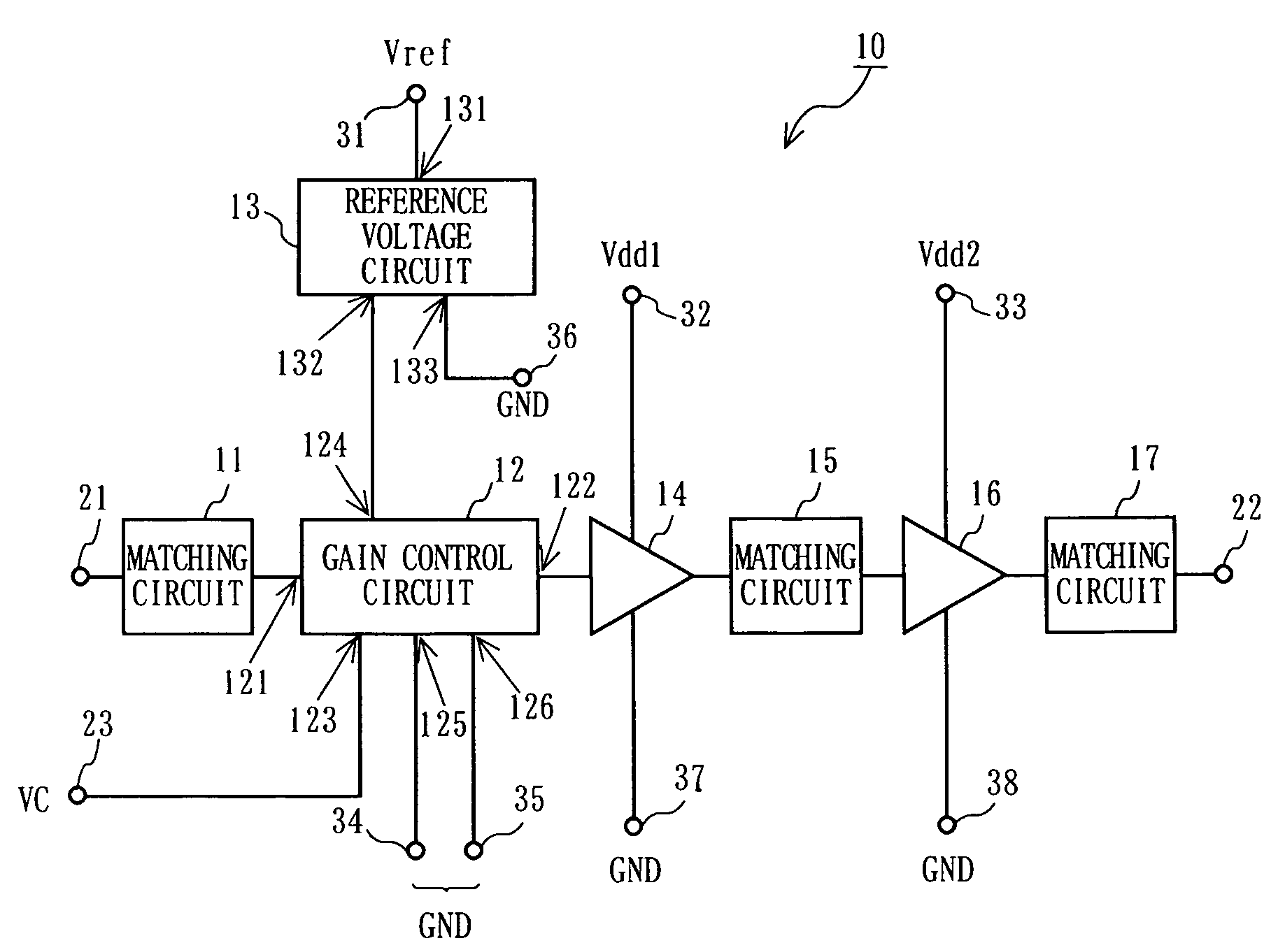
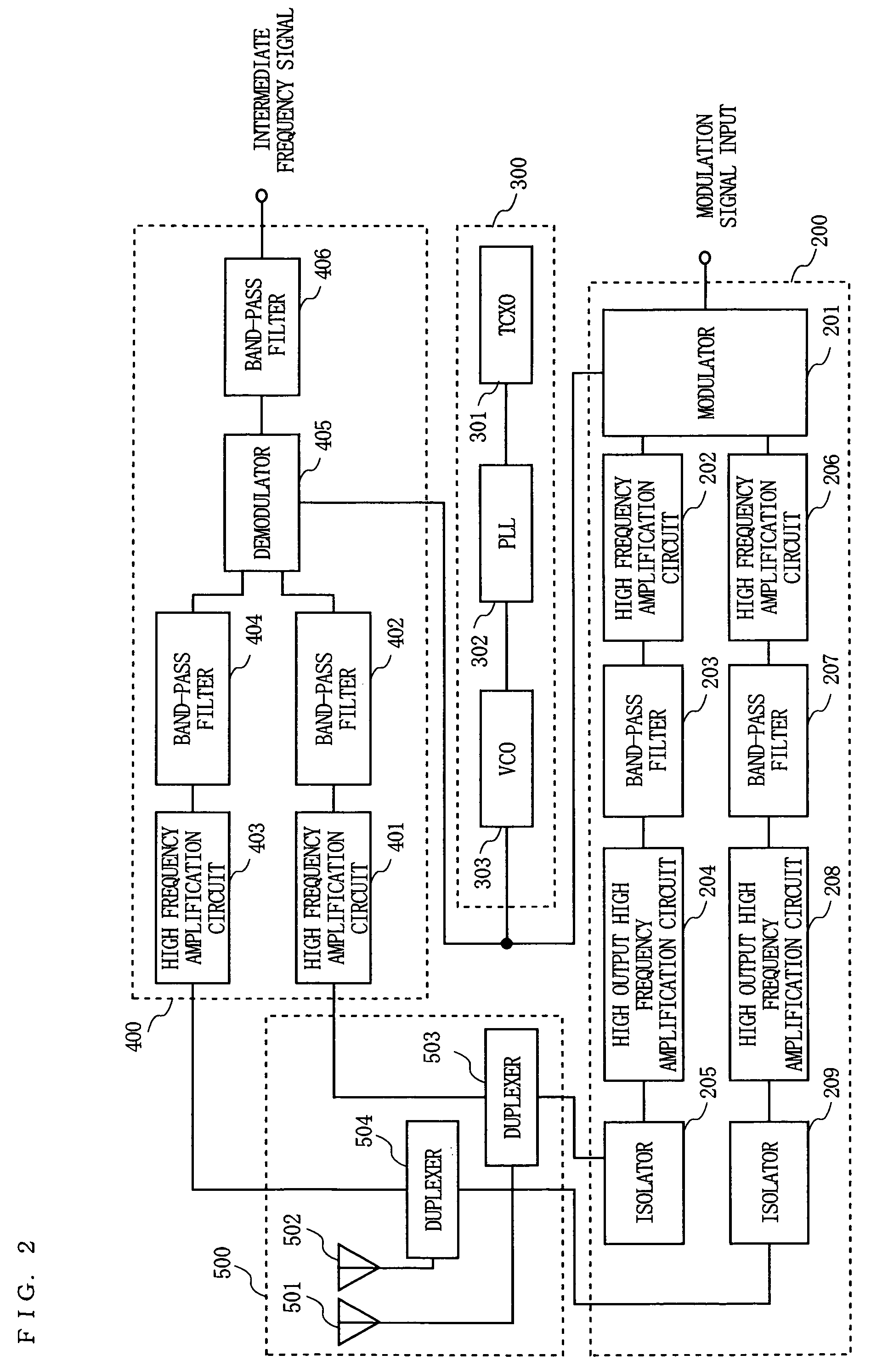
[0071]FIG. 1 is a block diagram showing a structure of a high frequency amplification circuit 10 according to a first embodiment of the present invention. FIG. 2 is a block diagram showing a structure of a wireless section of a cellular phone terminal including the high frequency amplification circuit 10 shown in FIG. 1. The high frequency amplification circuit 10 shown in FIG. 1 is used as a high frequency amplification circuit 202 and / or a high frequency amplification circuit 206 in the wireless section of the cellular phone terminal shown in FIG. 2. In other words, the cellular phone terminal according to this embodiment is the mobile communication terminal shown in FIG. 2 in which at least one of the high frequency amplification circuits 202 and 206 has the structure of the high frequency amplification circuit 10 shown in FIG. 1.

[0072]Before describing the high frequency amplification circuit 10 in detail, the wireless section of the cellular phone terminal shown in FIG. 2 will ...

second embodiment

[0114]FIG. 8 is a block diagram showing a structure of a high frequency amplification circuit 18 according to a second embodiment of the present invention. Like the high frequency amplification circuit 10 according to the first embodiment, the high frequency amplification circuit 18 shown in FIG. 8 is used as the high frequency amplification circuit 202 and / or the high frequency amplification circuit 206 in the cellular phone terminal shown in FIG. 2. In other words, a cellular phone terminal according to this embodiment is the cellular phone terminal shown in FIG. 2 in which at least one of the high frequency amplification circuits 202 and 206 has the structure of the high frequency amplification circuit 18 shown in FIG. 8. Among the elements in this embodiment, elements identical to those in the first embodiment bear identical reference numerals thereto, and descriptions thereof will be omitted.

[0115]The high frequency amplification circuit 18 is different from the high frequency ...

third embodiment

[0159]FIG. 13 is a block diagram showing a structure of a high frequency amplification circuit 600 according to a third embodiment of the present invention. Like the high frequency amplification circuit 10 according to the first embodiment, the high frequency amplification circuit 600 shown in FIG. 13 is used as the high frequency amplification circuit 202 and / or the high frequency amplification circuit 206 in the cellular phone terminal shown in FIG. 2. In other words, a cellular phone terminal according to this embodiment is the cellular phone terminal shown in FIG. 2 in which at least one of the high frequency amplification circuits 202 and 206 has the structure of the high frequency amplification circuit 600 shown in FIG. 13. Among the elements in this embodiment, elements identical to those in the first embodiment bear identical reference numerals thereto, and descriptions thereof will be omitted.

[0160]The high frequency amplification circuit 600 is different from the high freq...


PUM


Abstract

A gain control circuit 12 comprises an FET 41 operating as a variable resistor. A gate terminal of the FET 41 is supplied with a control voltage VC applied to a gain control terminal 23. A source terminal and a drain terminal of the FET 41 are supplied with a reference voltage Vref1 obtained by a reference voltage circuit 13. The reference voltage Vref1 is controlled so as to compensate for a variation in the threshold voltage of the FET 41. The resistance value of the FET 41 is changed in accordance with the control voltage VC, and thus the gain of the high frequency amplification circuit 10 is also continuously changed.

Description

BACKGROUND OF THE INVENTION[0001]1. Field of the Invention[0002]The present invention relates to a high frequency amplification circuit and a mobile communication terminal using the same, and more specifically to a high frequency amplification circuit provided in a high frequency circuit block or the like of a transmission section of a mobile communication terminal for performing gain control in accordance with a given control voltage, and the mobile communication terminal using the same.[0003]2. Description of the Background Art[0004]Recently, in the field of mobile communication, composite cellular phone terminals compatible to a plurality of communication systems are becoming main stream mobile communication terminals. Examples of such composite cellular phone terminals are compatible to the PDC (Personal Digital Cellular) system and the W-CDMA (Wide band Code Division Multiple Access) system. The PDC system has an advantage of providing a wide service area, and the W-CDMA system...

Claims


Application Information

Patent Timeline
Patent Type & Authority Patents(United States)
IPC IPC(8): H04B1/04
CPCH03G1/007
Inventor NAKAYAMA, MASAOTAKAGI, TSUNEHIROINAMORI, MASAHIKOMOTOYOSHI, KANAME
Owner COLLABO INNOVATIONS INC
Why Eureka
Try Eureka