Electronic component with die and passive device

a passive device and electronic component technology, applied in the direction of semiconductor devices, semiconductor/solid-state device details, electrical devices, etc., can solve the problems of increasing reducing the distance of the signal transmission path, and increasing the delay and attenuation of the signal

Inactive Publication Date: 2008-03-18
QUALCOMM INC
View PDF13 Cites 37 Cited by
  • Summary
  • Abstract
  • Description
  • Claims
  • Application Information

AI Technical Summary

Problems solved by technology

As a result, this method fails to reduce the distance of the signal transmission path but in fact increase the signal path distance.
This will increase signal delay and attenuation and decrease the performance of the chip.
Although WLCSP can greatly reduce the signal path distance, it is still very difficult to accommodate all the bonding points on the die surface as the integration of die and internal components gets higher.
The pin count on the die increases as integration gets higher so the redistribution of pins in an area array is difficult to achieve.
Even if the redistribution of pins is successful, the distance between pins will be too small to meet the pitch of a printed circuit board (PCB).

Method used


Image

  • Electronic component with die and passive device
  • Electronic component with die and passive device
  • Electronic component with die and passive device

Examples


first embodiment

[0043]According to the above, the present invention is a chip package structure with an organic substrate and a plurality of dies on the organic substrate. The external circuitry of the thin-film circuit layer allows the metal pads of the die to fan out. By forming bonding pads corresponding to the metal pads of the dies such as solders balls, bumps, or pins as the signal input terminals, the distance of the signal path is effectively decreased. As a result, signal delay and attenuation are reduced to increase performance of the die.

[0044]The present invention uses existing technology on and equipment for fabricating PCB for the fabrication of the organic substrate by heat pressing a plurality of insulating core boards. Alternatively, the organic substrate can also be fabricated in large volume by injection molding. As a result of the low fabrication and material cost of the organic substrate, the cost of chip packaging is also lowered.

[0045]The second embodiment of the present inve...

second embodiment

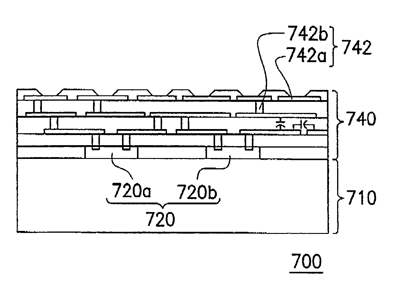
[0049]the present invention is an organic substrate with a plurality of inwardly protruded areas for inlaying dies by adhering the backside of the dies to the bottom of the inwardly protruded areas and exposing the active surface of the dies. A thin-film circuit layer is formed on top of the dies and the organic substrate to fan out the metal pads of the dies by using the external circuitry of the thin-film circuit layer. Due to the inlay of the dies in the organic substrate, thinning of the thickness of the chip package structure is effectively achieved and the surface of the organic substrate provides enough planarity and support for the formation of the thin-film circuit layer.

[0050]The third embodiment of the present invention differs from the second embodiment of the present invention by using an integrated organic substrate with at least one organic layer and one heat conducting layer. FIG. 3A to 3C are schematic diagrams of the sectional view of the third embodiment illustrat...

third embodiment

[0054]the present invention is an integrated organic substrate with an organic layer with a plurality of openings and a heat conducting layer. The openings in the organic layer will form the inwardly protruded areas in the integrated organic substrate. The backside of the die adheres to the bottom of the inwardly protruded areas so the dies are inlayed in the inwardly protruded areas and exposing the active surface of the dies. This integrated organic substrate can efficiently dissipate heat from the dies to the outside because the bottom of the inwardly protruded area is the surface of the heat conducting material. The surface of the organic substrate provides enough planarity and support for the formation of the thin-film circuit layer.

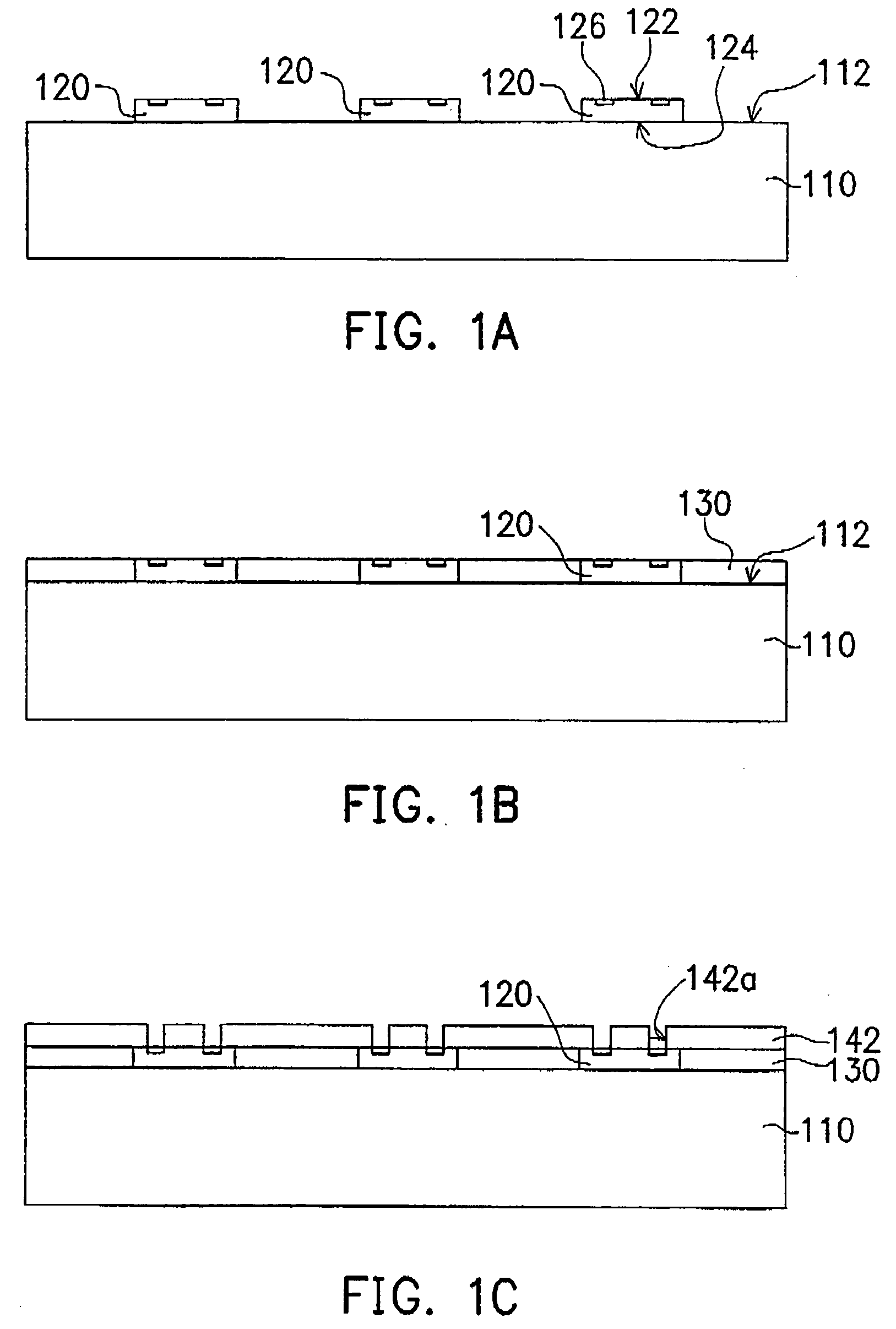
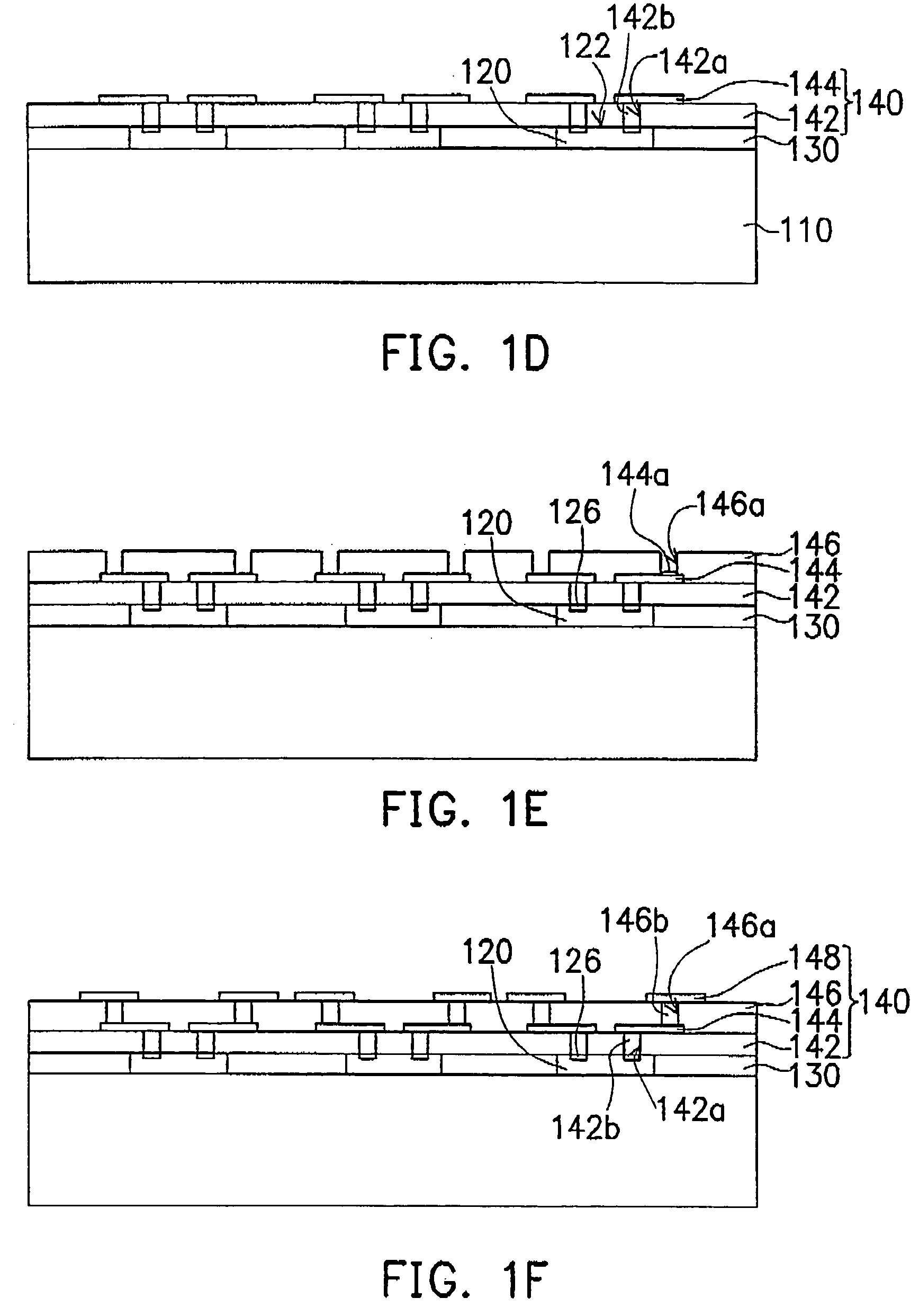
[0055]The fourth embodiment of the present invention is slightly different from the first three embodiments. FIG. 4A to 4E are schematic diagrams of the sectional view of the fourth embodiment illustrating the fabrication of the structure.

[0056]Plea...


PUM

PropertyMeasurementUnit
thicknessaaaaaaaaaa
thicknessaaaaaaaaaa
thicknessaaaaaaaaaa

Abstract

An integrated chip package structure and method of manufacturing the same is by adhering dies on an organic substrate and forming a thin-film circuit layer on top of the dies and the organic substrate. Wherein the thin-film circuit layer has an external circuitry, which is electrically connected to the metal pads of the dies, that extends to a region outside the active surface of the dies for fanning out the metal pads of the dies. Furthermore, a plurality of active devices and an internal circuitry is located on the active surface of the dies. Signal for the active devices are transmitted through the internal circuitry to the external circuitry and from the external circuitry through the internal circuitry back to other active devices. Moreover, the chip package structure allows multiple dies with different functions to be packaged into an integrated package and electrically connecting the dies by the external circuitry.

Description

CROSS-REFERENCE TO RELATED APPLICATION[0001]This application claims the priority benefit of Taiwan application serial no. 90133093, filed Dec. 31, 2001.[0002]This application is related to application Ser. No. 10 / 054,001, filed on Jan. 19, 2002, now U.S. Pat. No. 6,673,698; and related to application Ser. No. 10 / 690,350, filed on Oct. 21, 2003, and related to application Ser. No. 10 / 996,535, filed on Nov. 24, 2004, and related to application Ser. No. 10 / 996,537, filed on Nov. 24, 2004, and related to application Ser. No. 10 / 055,498, filed on Jan. 22, 2002, now U.S. Pat. No. 6,800,941; and related to application Ser. No. 10 / 454,972, filed on Jun. 4, 2003, and related to application Ser. No. 10 / 055,560, filed on Jan. 22, 2002, and related to application Ser. No. 10 / 638,018, filed on Aug. 8, 2003, and related to application Ser. No. 10 / 977,289, filed on Oct. 28, 2004, and related to application Ser. No. 10 / 055,568, filed on Jan. 22, 2002, and related to application Ser. No. 10 / 174,462,...

Claims


Application Information

Patent Timeline
Patent Type & Authority Patents(United States)
IPC IPC(8): H01L23/52H01L23/34H01L23/40H01L23/538H01L23/48H01L21/48H01L21/60H01L21/68H01L23/498
CPCH01L21/4857H01L23/49822H01L23/5389H01L24/19H01L24/97H01L21/6835Y10T29/5317H01L2221/68363H01L2221/68377H01L2224/04105H01L2224/20H01L2224/211H01L2224/97H01L2924/01029H01L2924/01078H01L2924/01079H01L2924/14H01L2924/15311H01L2924/19041H01L2924/19042H01L2924/19043Y10T29/5313H01L2924/1461H01L2224/0401H01L2224/92244H01L2224/73267H01L2224/32225H01L2224/12105H01L2924/01005H01L2924/01006H01L2924/01033H01L2924/014H01L2224/82H01L2224/83H01L2924/00H01L2924/12042H01L2924/15788
Inventor LEE, JIN-YUANLIN, MOU-SHIUNGHUANG, CHING-CHENG
Owner QUALCOMM INC
Why Eureka
Try Eureka