Semiconductor light emitting devices including flexible film having therein an optical element

a technology flexible films, which is applied in the direction of discharge tubes/lamp details, discharge tubes luminescnet screens, electric discharge lamps, etc., can solve the problems of high assembly costs, time-consuming and/or failures, and the packaging of semiconductor light emitting devices may be more expensive than the semiconductor light emitting element itself, so as to reduce shadowing

Active Publication Date: 2008-04-08
CREELED INC
View PDF41 Cites 117 Cited by
  • Summary
  • Abstract
  • Description
  • Claims
  • Application Information

AI Technical Summary

Benefits of technology

[0007]Many different configurations of optical elements may be provided according to various embodiments of the present invention. In some embodiments, the optical element includes (i.e., comprises) a lens. In other embodiments, the optical element includes a prism. In other embodiments, the flexible film includes a first face adjacent the substrate and a second face remote from the substrate, and the optical element includes a first optical element on the first face, and a second optical element on the second face, both of which are located such that the light emitting element emits light through the first optical element and the second optical element. In some embodiments, the optical element includes phosphor and / or other optical emission enhancing and / or converting elements. In still other embodiments, the optical element includes an optical scattering element. Combinations and subcombinations of these and / or other optical elements also may be provided. Moreover, an optical coupling media may be provided between the optical element and the semiconductor light emitting element in any of these embodiments.
[0010]Some embodiments of the present invention may be configured to incorporate phosphor into the semiconductor light emitting device. In some embodiments, phosphor is provided on the flexible film between the lens and the semiconductor light emitting element. In other embodiments, the lens includes a concave inner surface adjacent the semiconductor light emitting element, and the phosphor includes a conformal phosphor layer on the concave inner surface. In yet other embodiments, the optical element includes a lens that overlies the cavity and protrudes away from the cavity, the flexible film further includes a protruding element between the lens and the light emitting element that protrudes towards the cavity, and a conformal phosphor coating is provided on the protruding element. Combinations and subcombinations of these and / or other configurations of phosphor also may be provided. Moreover, an optical coupling media may be provided between the phosphor and the semiconductor light emitting element in any of these embodiments.
[0011]In still other embodiments of the present invention, the semiconductor light emitting element includes a wire that extends towards the flexible substrate. In some of these embodiments, the optical element includes a prism that is configured to reduce shadowing by the wire, of the light that is emitted from the semiconductor light emitting element.

Problems solved by technology

Unfortunately, the packaging for a semiconductor light emitting device may be costly and, in some cases, more costly than the semiconductor light emitting element itself.
Moreover, the assembly process also may be costly, time consuming and / or subject to failures.

Method used


Image

  • Semiconductor light emitting devices including flexible film having therein an optical element
  • Semiconductor light emitting devices including flexible film having therein an optical element
  • Semiconductor light emitting devices including flexible film having therein an optical element

Examples


Embodiment Construction

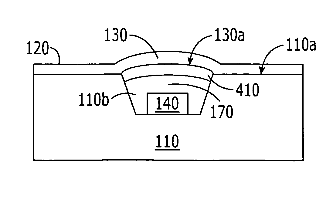
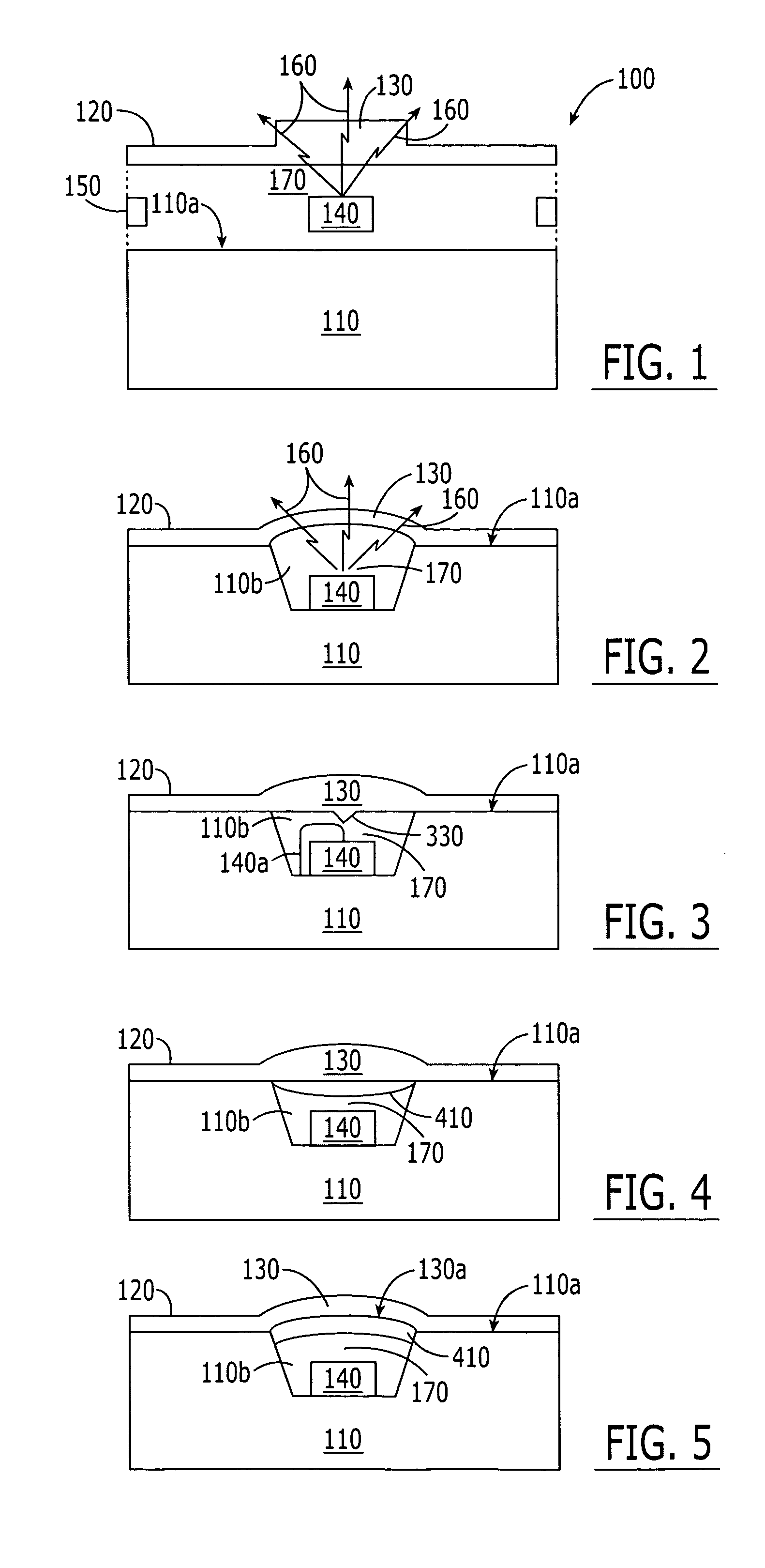
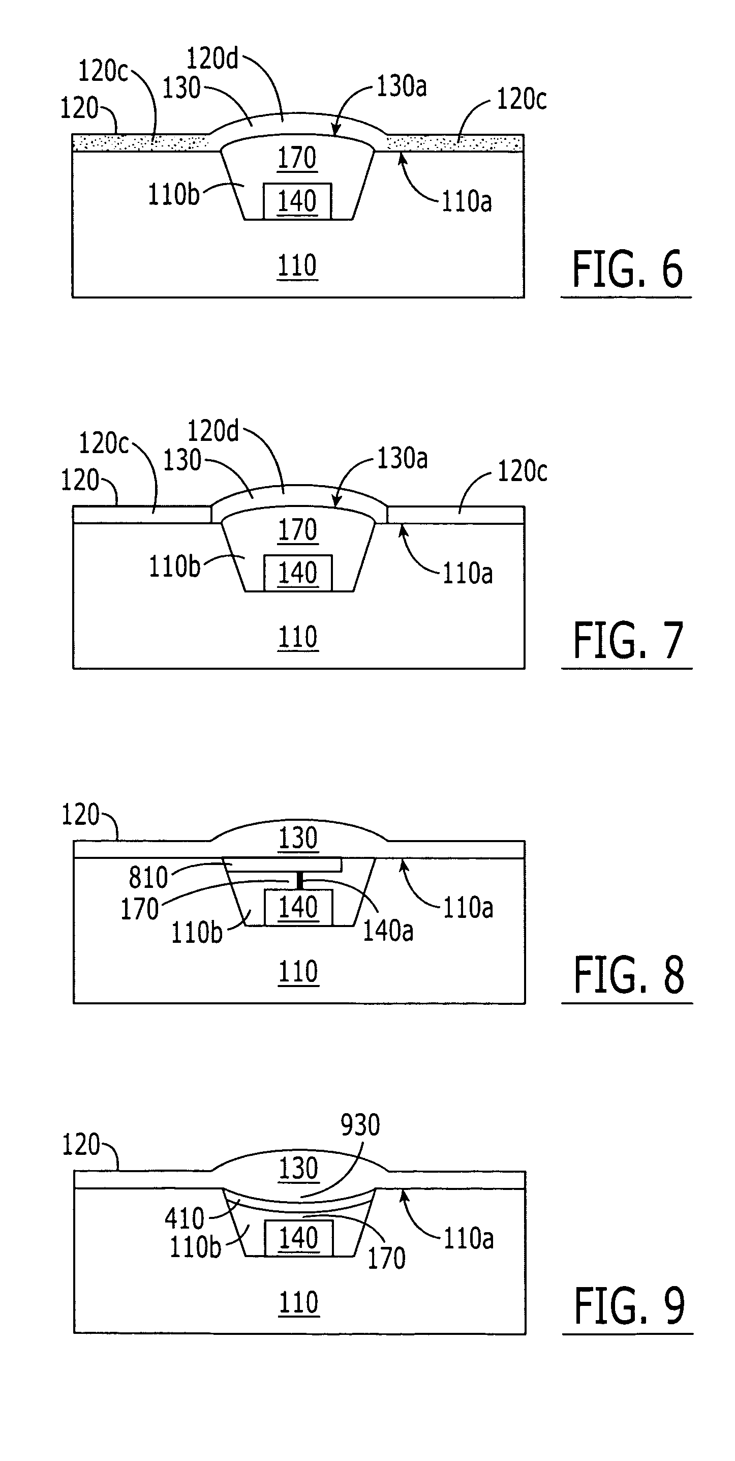
[0016]The present invention now will be described more fully hereinafter with reference to the accompanying drawings, in which embodiments of the invention are shown. This invention may, however, be embodied in many different forms and should not be construed as limited to the embodiments set forth herein. Rather, these embodiments are provided so that this disclosure will be thorough and complete, and will fully convey the scope of the invention to those skilled in the art. In the drawings, the size and relative sizes of layers and regions may be exaggerated for clarity. Like numbers refer to like elements throughout.

[0017]It will be understood that when an element such as a layer, region or substrate is referred to as being “on” another element, it can be directly on the other element or intervening elements may also be present. It will be understood that if part of an element, such as a surface, is referred to as “inner,” it is farther from the outside of the device than other pa...


PUM


Abstract

Semiconductor light emitting devices include a substrate having a face, a flexible film that includes therein an optical element, on the face, and a semiconductor light emitting element between the substrate and the flexible film and configured to emit light through the optical element. The face can include a cavity therein, and the semiconductor light emitting element may be in the cavity. The flexible film extends onto the face beyond the cavity, and the optical element overlies the cavity.

Description

FIELD OF THE INVENTION[0001]This invention relates to semiconductor light emitting devices and fabricating methods therefor, and more particularly to packaging and packaging methods for semiconductor light emitting devices.BACKGROUND OF THE INVENTION[0002]Semiconductor light emitting devices, such as Light Emitting Diodes (LEDs) or laser diodes, are widely used for many applications. As is well known to those having skill in the art, a semiconductor light emitting device includes a semiconductor light emitting element having one or more semiconductor layers that are configured to emit coherent and / or incoherent light upon energization thereof. It is also known that the semiconductor light emitting element generally is packaged to provide external electrical connections, heat sinking, lenses or waveguides, environmental protection and / or other functions for the semiconductor light emitting device. Packaging may be provided, at least in part, by at least partially surrounding the semi...

Claims


Application Information

Patent Timeline
Patent Type & Authority Patents(United States)
IPC IPC(8): H01L29/40H01L33/50H01L33/54H01L33/60H01L33/62
CPCH01L33/54H01L33/60H01L33/507H01L33/62H01L2924/0002H01L2924/00H01L33/58H01L33/486H01L33/48
Inventor NEGLEY, GERALD H.
Owner CREELED INC
Why Eureka
Try Eureka