
Illumination control circuit

a control circuit and circuit technology, applied in the direction of electric variable regulation, process and machine control, instruments, etc., can solve the problems of large loss of collectors of transistors and rapid increase of collector losses of driving transistors, and achieve the effect of reducing the load on the driving elemen

Inactive Publication Date: 2008-04-08
PIONEER CORP
View PDF9 Cites 0 Cited by
  • Summary
  • Abstract
  • Description
  • Claims
  • Application Information

AI Technical Summary

Benefits of technology

[0009]In the above-described conventional illumination adjustment circuit, the constant voltage (V2) generated in the zener diode (D1) is used as a reference voltage, and such a constant voltage (V2) is switched and smoothened so as to generate a DC voltage (VB) for adjusting a potential at the base of the driving transistor (Q1). As a result, it becomes possible to perform an adjustment on the illuminating lamp (FL) to ensure a constant illuminance, without being influenced by a voltage fluctuation of the power supply (Vcc).
[0012]The present invention has been accomplished in view of the above-discussed conventional problem and it is an object of the invention to provide an illumination control circuit having a driving element for driving an illuminating lamp, a light emitting lamp, a light emission element or the like, thereby ensuring an improved illumination control circuit capable of reducing a load on the driving element, even if there has been a fluctuation or the like on the power source voltage.

Problems solved by technology

However, when a fluctuation occurs in the power supply (Vcc) and a voltage level rises up, since the potential at the base of the driving transistor (Q1) is maintained at a constant level by virtue of the DC voltage (VB), a voltage between the collector and the base of the driving transistor (Q1) will also rise, resulting in a problem that the transistor's collector loss is large.
In particular, when driving / controlling an illuminating lamp (FL) which requires a large electric power consumption, once a voltage level of a power supply (Vcc) rises up, a load on the driving transistor (Q1) will increase, thus causing a rapid increase in the collector loss of the driving transistor (Q1), or a deterioration in the characteristic of the driving transistor (Q1), which is caused possibly due to a heat generation, hence bringing about a problem of causing a wound or the like.

Method used


Image

  • Illumination control circuit
  • Illumination control circuit
  • Illumination control circuit

Examples


embodiment 1

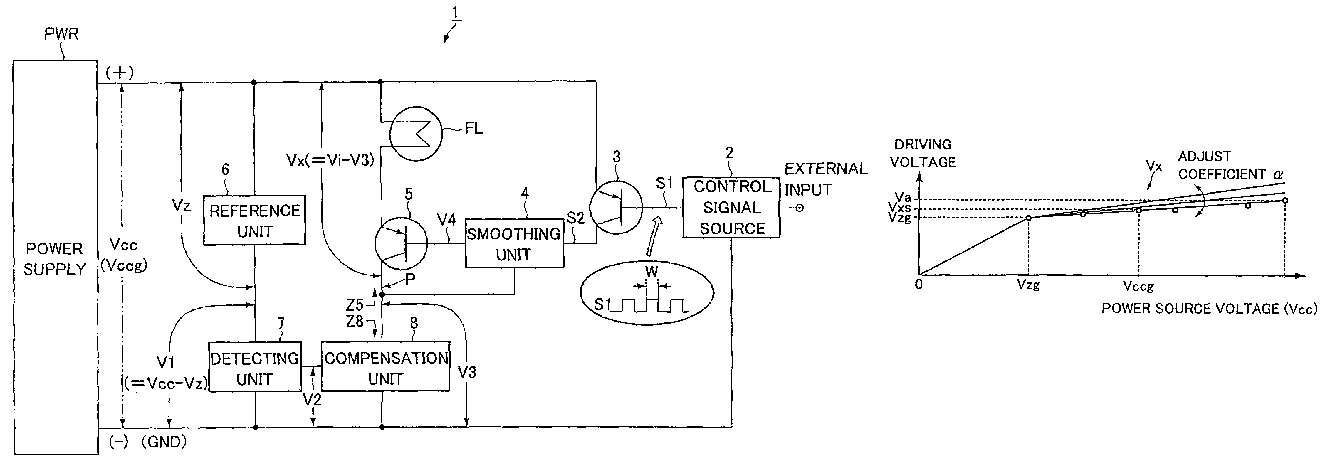
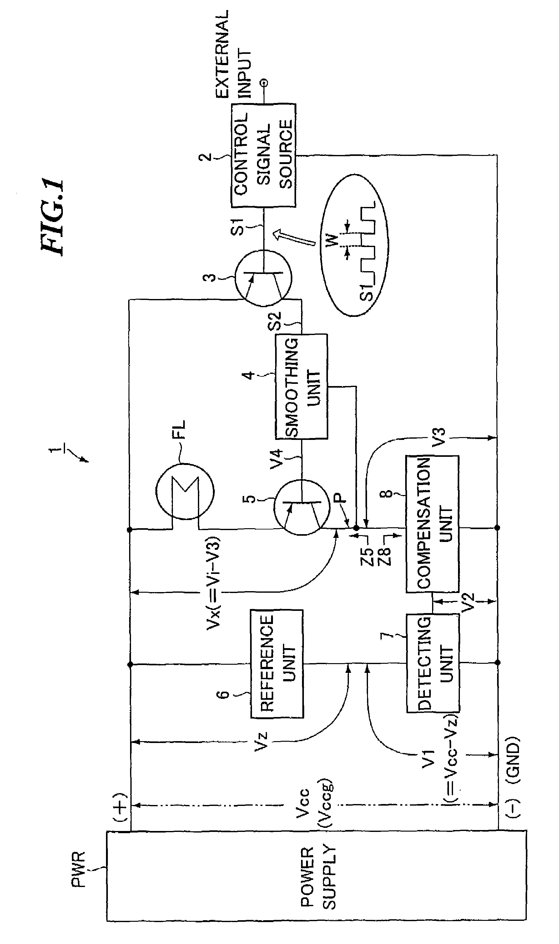
[0022]FIG. 1 is a circuit diagram showing a structure of an illumination control circuit according to a first embodiment of the present invention.

[0023]As shown in FIG. 1, the illumination control circuit 1 comprises a control signal source 2, a switching element 3 serving as a control element, a smoothing unit 4, a driving element 5, a reference unit 6, a detecting unit 7, and a compensating unit 8. When the illumination control circuit 1 is connected to a power source PWR such as a vehicle battery mounted in a vehicle, the illumination control circuit 1 will operate to control the illuminance or the light intensity of an illuminating lamp, a light emitting lamp and a light emission element FL which all receive an electric power supplied from the power source PWR and thus emit light.

[0024]In the following, for an easy description, an illuminating lamp, a light emitting lamp and a light emission element will all be simply referred to as “light emission element”.

[0025]The control sig...

embodiment 2

[0064]Next, description will be given to explain an illumination control circuit formed according to a second embodiment of the present invention, with reference to FIG. 3. Here, FIG. 3 is a circuit diagram showing a structure of the illumination control circuit 1 of the present embodiment, with the elements identical or equal to those in FIG. 1 being represented by the same reference numerals.

[0065]As shown in FIG. 3, the illumination control circuit 1 comprises a control signal source 2, a switching element 3 serving as a control unit, a smoothing unit 4, a driving element 5, a reference unit 6, a detecting unit 7, and a compensation unit 10.

[0066]Similar to the first embodiment shown in FIG. 1, the control signal source 2 is formed of an oscillating circuit which outputs the PWM signal S1, and capable of variably adjusting the pulse width W of the PWM signal S1 by virtue of an external operation inputted thereto.

[0067]The switching element 3 performs a switching operation in acco...

example 1

[0095]Next, with reference to FIG. 4, description will be given to explain in more detail an example of the illumination control circuit 1 formed according to the first embodiment of the present invention.

[0096]FIG. 4 is a circuit diagram showing a structure of the illumination control circuit of the present embodiment, with elements identical or equal to those in FIG. 1 being represented by the same reference numerals.

[0097]As shown in FIG. 4, similar to the illumination control circuit of the embodiment shown in FIG. 1, this illumination control circuit 1 comprises: a control signal source 2, a switching element 3, a smoothing unit 4, a driving element 5, a reference unit 6, a detecting unit 7, and a compensation unit 8.

[0098]The control signal source 2 comprises an oscillating circuit 2a outputting PWM signal S0, NPN transistor 2f, and bias resistors 2b-2e. The NPN transistor 2f invert-amplifies the PWM signal S0. The invert-amplified PWM signal S1 is then supplied to the base of...


PUM


Abstract

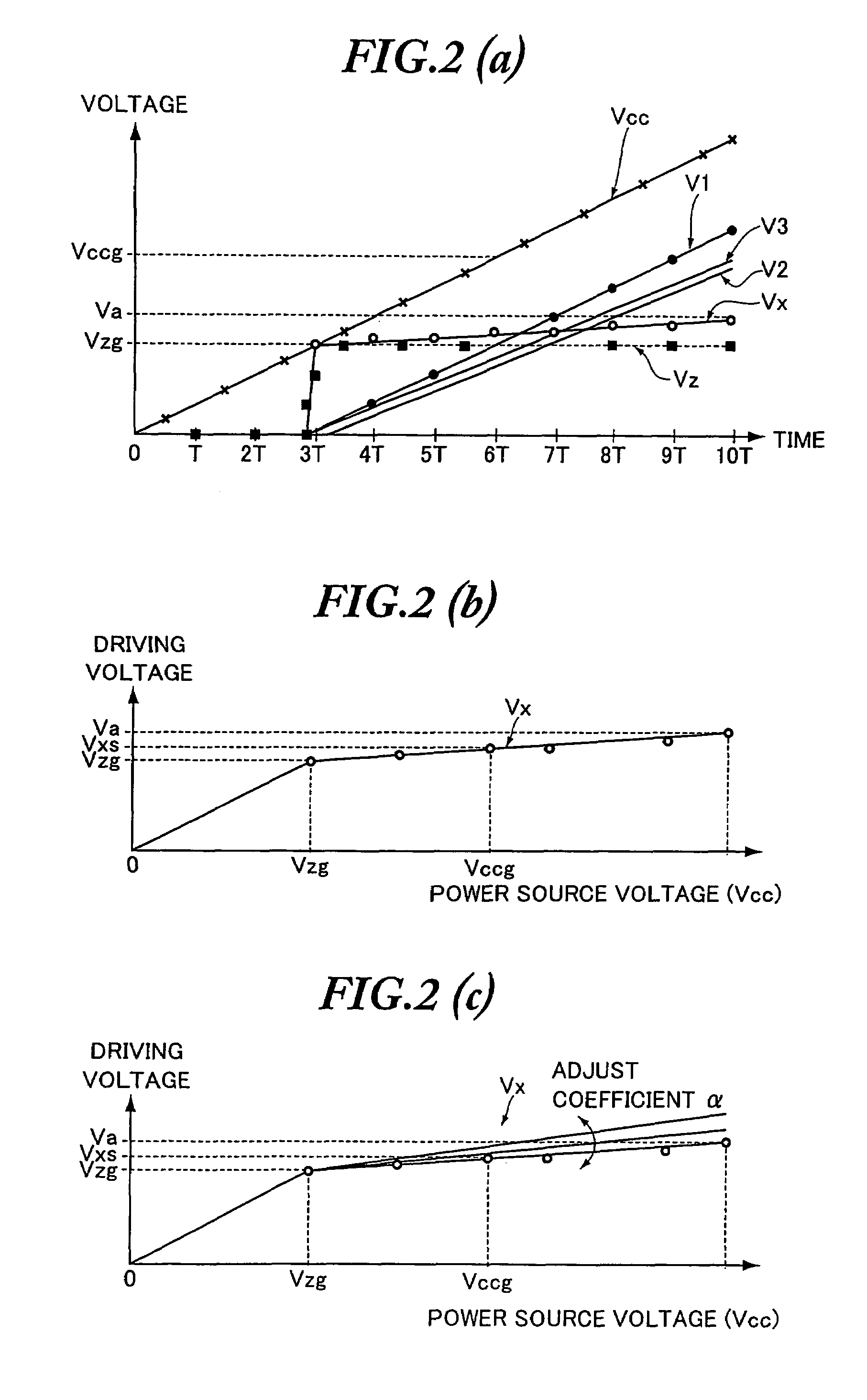
It is an object of the invention to provide an improved illumination control circuit comprising a light emission element FL, a driving element 5 for driving the light emission element FL, and a compensation unit 8 are connected in series with respect to a power source voltage Vcc. Further, a reference unit 6 for generating a constant voltage Vz and a detecting unit 7 are connected in series with respect to the power source voltage Vcc. The detecting unit 7 is provided for detecting a differential voltage V1 between the power source voltage Vcc and the constant voltage Vz. Once there is a change in the power source voltage Vcc, the detecting unit 7 detects a voltage change of the power source voltage Vcc in accordance with the differential voltage V1, generates a detection voltage V2 formed by dividing the differential voltage V1, while the compensation unit 8 generates a compensation voltage V3 following the detection voltage V2, thereby inhibiting a change of a driving voltage Vx applied between two ends of the light emission element FL and the driving element 5, in response to a change of the power source voltage Vcc.

Description

CROSS-REFERENCE TO RELATED APPLICATION[0001]This application is a National Stage entry of International Application No. PCT / JP2005 / 005948, filed Mar. 29, 2005, claiming the priority benefit of Japan Application No. 2004-105297 filed on Mar. 31, 2004; the entire specification claims and drawings of which are incorporated herewith by reference.TECHNICAL FIELD[0002]The present invention relates to an illumination control circuit which controls so-called brightness such as an illuminance and a light intensity of an illuminating lamp, a light emitting lamp, and a light emission element or the like.TECHNICAL BACKGROUND[0003]Japanese Unexamined Patent Application Publication No. Hei 11-233276 has disclosed an illumination control circuit (an illumination adjustment circuit) which drives an illuminating lamp for illuminating car audio device and adjusts its illuminance.[0004]As shown in FIG. 1 of the above-mentioned patent document, the illumination adjustment circuit comprises a resistor (...

Claims


Application Information

Patent Timeline
Patent Type & Authority Patents(United States)
IPC IPC(8): H05B37/02H05B41/16H05B39/04
CPCH05B39/047Y02B20/144Y02B20/00
Inventor INOUE, TAKAO
Owner PIONEER CORP
Learn More