Method for preparing an optical active layer with 1~10 nm distributed silicon quantum dots

a distributed silicon quantum dots and active layer technology, applied in the field of preparing an optical active layer with 1 10 nm distributed silicon quantum dots, can solve the problem of poor red light reproducibility

Inactive Publication Date: 2008-04-15
INST NUCLEAR ENERGY RES ROCAEC
View PDF6 Cites 20 Cited by
  • Summary
  • Abstract
  • Description
  • Claims
  • Application Information

AI Technical Summary

Problems solved by technology

However, deficient red spectrum of emitting causes poor reproducibility of red light.

Method used


Image

  • Method for preparing an optical active layer with 1~10 nm distributed silicon quantum dots
  • Method for preparing an optical active layer with 1~10 nm distributed silicon quantum dots
  • Method for preparing an optical active layer with 1~10 nm distributed silicon quantum dots

Examples


Embodiment Construction

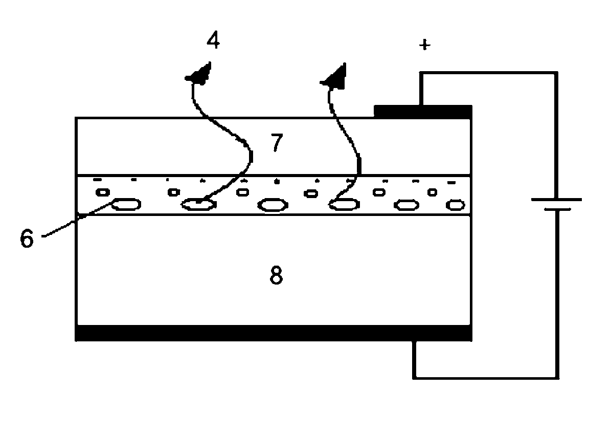
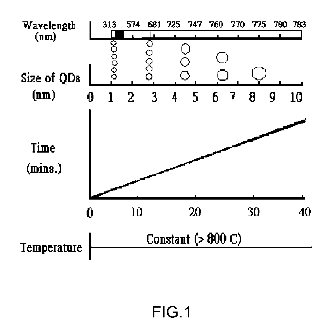
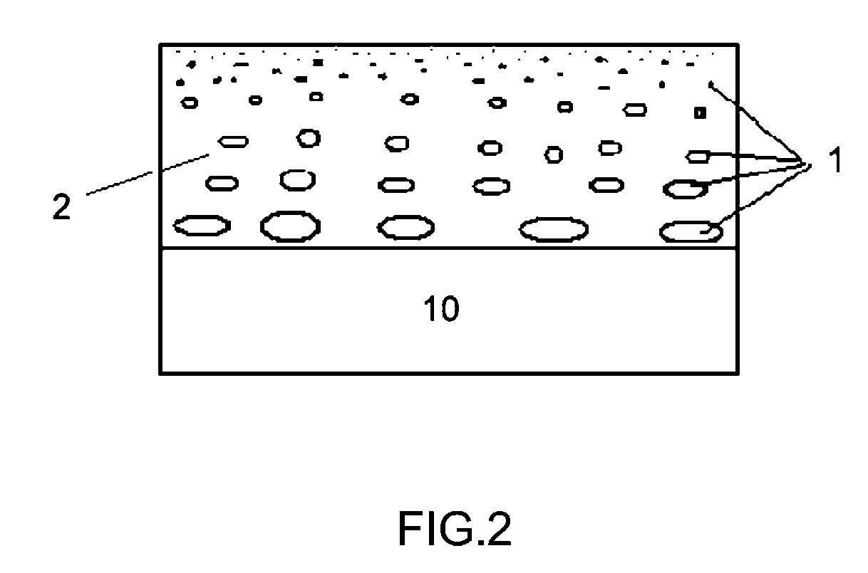
[0016]FIG. 1 shows the silicon quantum dots, which are formed during the deposition or growth of sub-stoichiometric silicon nitrite under certain time and temperature conditions; the distribution profile of grain size from the interface of said film and substrate to the surface of film is corresponding to from large to small grains of quantum dots; the distribution curve is in linear increment; the size of said silicon quantum dots can be controlled within 1˜10 nm diameter by modulating temperature and time of deposition and the ratio of silicon and nitrogen; such size of silicon quantum dots characterized by 1.5˜4.0 eV bandgap, and may generate spectrum within 300˜700 nm wavelength of white fluorescent light.

[0017]The substrate with deposited or grown sub-stoichiometric silicon nitrite film then put into furnace, and maintain at another annealing temperature and time under nitrogen environment for carry out all nucleation and growth of silicon nanocrystals, as well as curing proces...


PUM


Abstract

The present invention relates to a method for preparing an optical active layer with 1˜10 nm distributed silicon quantum dots, it adopts high temperature processing and atmospheric-pressure chemical vapor deposition (APCVD), and directly deposit to form a silicon nitrite substrate containing 1˜10 nm distributed quantum dots, said distribution profile of quantum dot size from large to small is corresponding to from inner to outer layers of film respectively, and obtain a 400˜700 nm range of spectrum and white light source under UV photoluminescence or electro-luminescence.

Description

BACKGROUND OF THE INVENTION[0001]Current major white light emission is blue light LED plus yellow yttrium aluminum garnet (YAG) phosphor, these patents are beneficial to Nichia Chemical Corporation and German OSRAM Opto Semiconductors, such as YAG white LED patent (U.S. Pat. No. 6,066,861) for Nichia Chemical Corporation and white LED patent (U.S. Pat. No. 6,066,861) for German OSRAM Opto Semiconductors. Lite-on Electronics Co. Ltd., Everlight Electronics Co. Ltd. and Harvatek Corporation are authorized by OSRAM Opto Semiconductors since the end of 2003. However, deficient red spectrum of emitting causes poor reproducibility of red light.[0002]For improve luminous efficiency of phosphors, Lumileds Lighting Corporation and Sandia National Laboratory (SNL) co-develop quantum dot phosphor technology (U.S. Pat. No. 6,501,091) in National Solid State Lighting Initiative of Department of Energy (DOE).[0003]Currently, it is gradually paying respect to use silicon quantum dots for light emi...

Claims


Application Information

Patent Timeline
Patent Type & Authority Patents(United States)
IPC IPC(8): H01L21/00
CPCB82Y10/00C09K11/0883C09K11/59H01L33/34Y02B20/181H01L33/504Y10S438/962Y10S977/774Y02B20/00
Inventor YANG, TSUN NENGLAN, SHAN MING
Owner INST NUCLEAR ENERGY RES ROCAEC
Why Eureka
Try Eureka