Semiconductor stacked die/wafer configuration and packaging and method thereof
a technology of stacked die/wafer and semiconductor, applied in the field of semiconductor devices, can solve the problems of increased die temperature, increased leakage power consumption, and slower operating speed
- Summary
- Abstract
- Description
- Claims
- Application Information
AI Technical Summary
Benefits of technology
Problems solved by technology
Method used
Image
Examples
Embodiment Construction
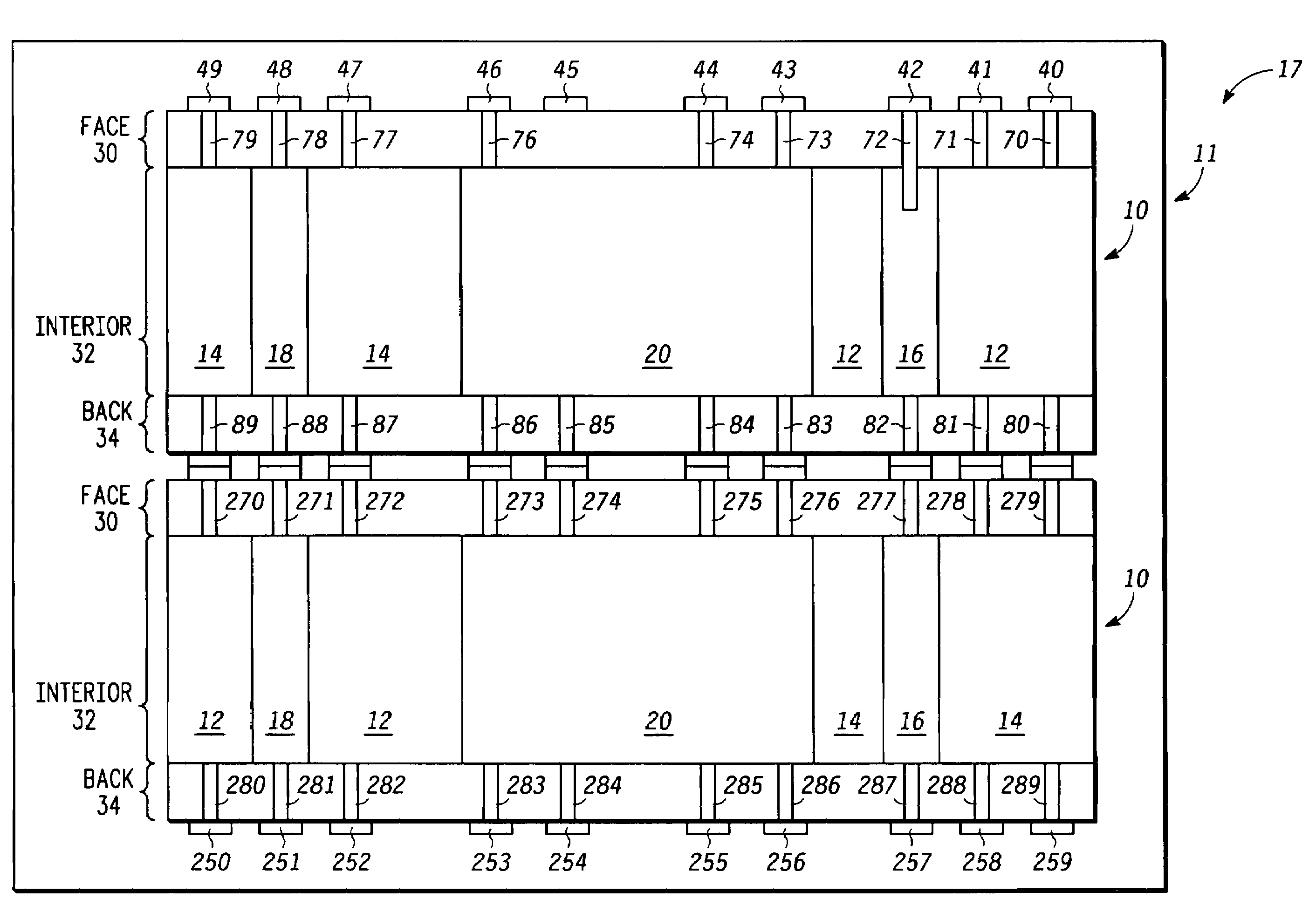
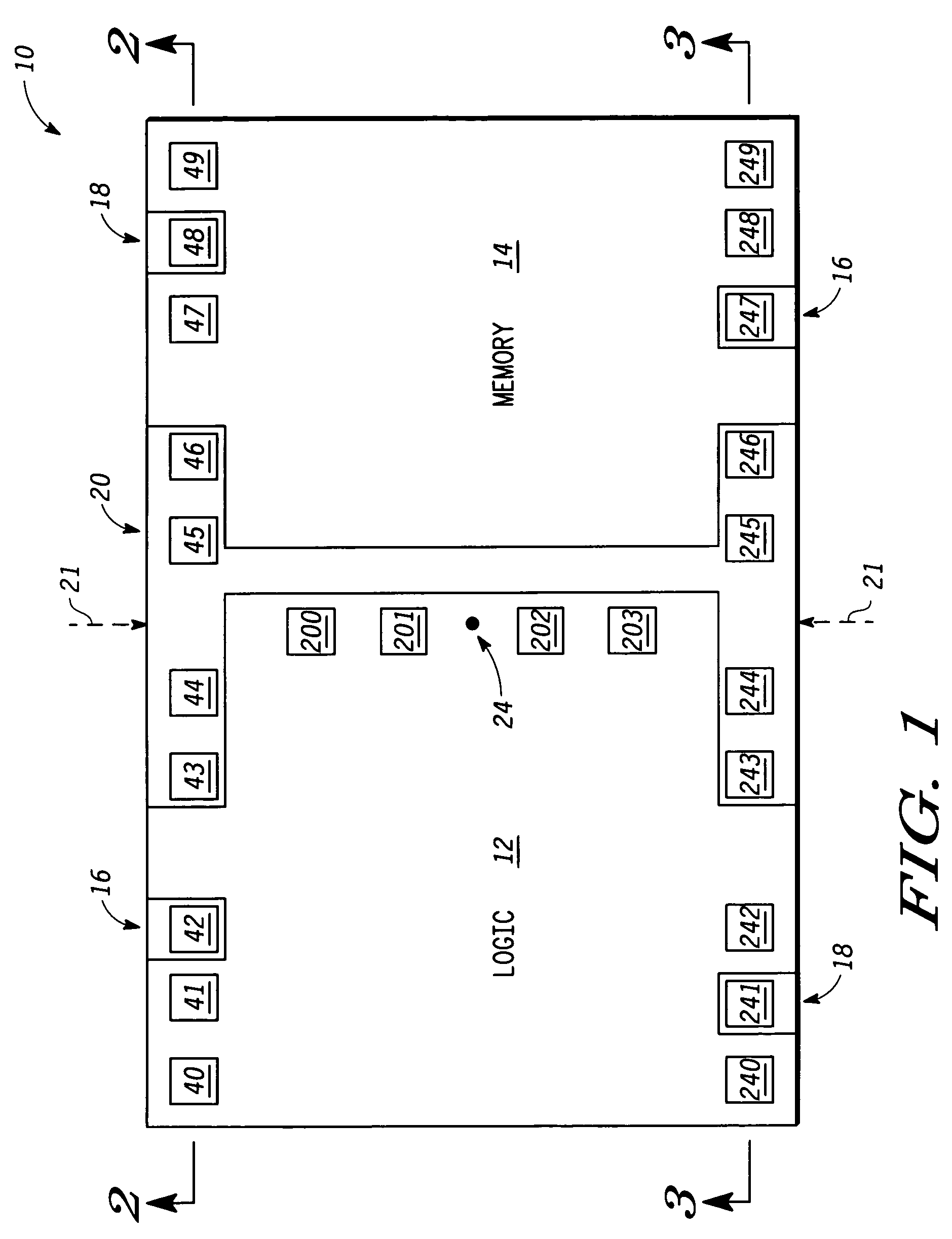
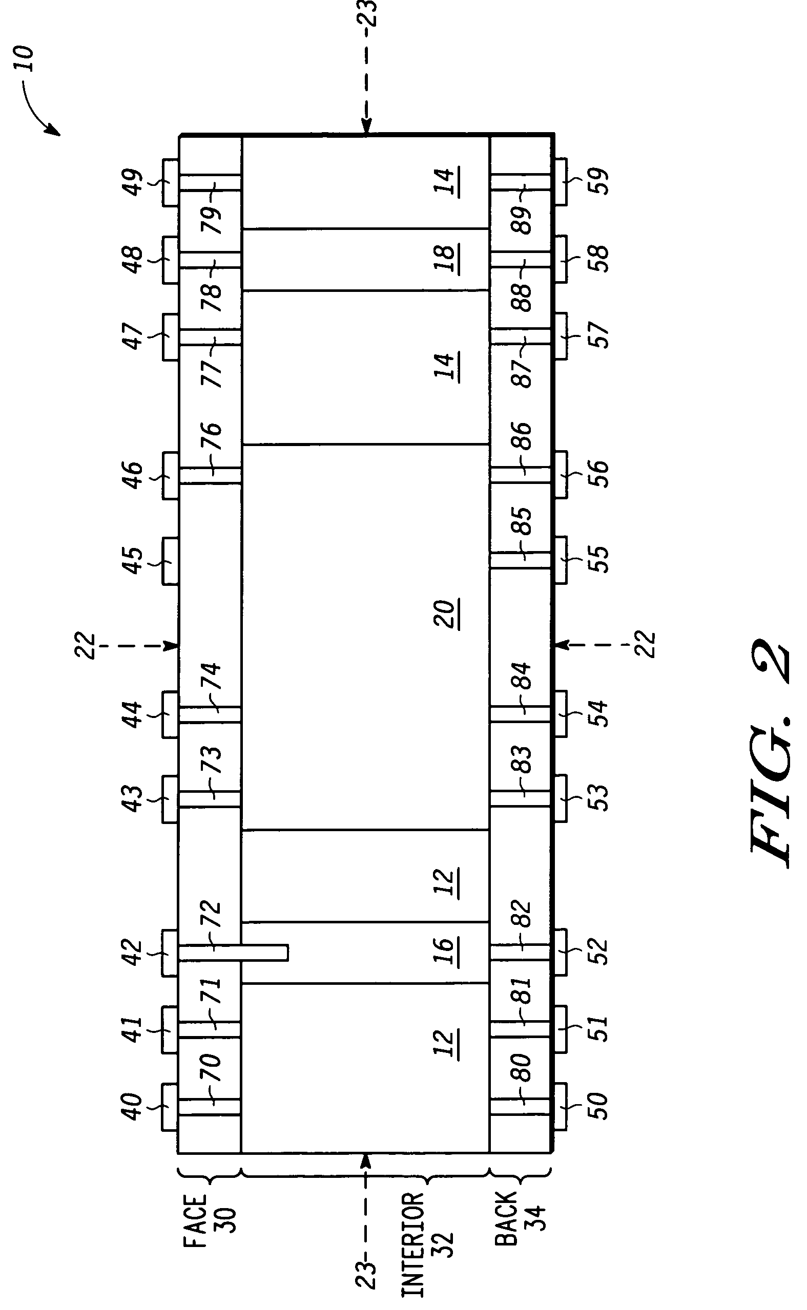
[0017]The present invention utilizes reciprocal design symmetry such that vertically integrated die can be fabricated using the same reticle set or substantially the same reticle set. As used here in the term ‘reciprocal design symmetry’ refers to a design which has the property that a first integrated circuit having such a design layout can be combined with a second integrated circuit of the same (or substantially the same) design layout by rotating or flipping the second integrated circuit and then placing it on top of the first integrated circuit (in its original orientation) such that connection of the adjacent contacts on the surfaces of the first and second integrated circuits completes a desired circuit which included circuit elements of both the first and second integrated circuits. The layouts of both the first and second integrated circuits are then defined to be ‘reciprocal circuit layouts’ of each other. Furthermore, the second integrated circuit following the rotation o...
PUM
 Abstract
Description
Claims
Application Information
 - R&D Engineer
- R&D Manager
- IP Professional
- Industry Leading Data Capabilities
- Powerful AI technology
- Patent DNA Extraction
Browse by: Latest US Patents, China's latest patents, Technical Efficacy Thesaurus, Application Domain, Technology Topic, Popular Technical Reports.
© 2024 PatSnap. All rights reserved.Legal|Privacy policy|Modern Slavery Act Transparency Statement|Sitemap|About US| Contact US: help@patsnap.com


