Reducing noise and/or power consumption in a switched capacitor amplifier sampling a reference voltage

a technology of switching capacitors and amplifiers, applied in the direction of amplifiers with semiconductor devices/discharge tubes, amplifiers with low noise, etc., can solve the problems of common mode voltage, error or non-linearity in the digital bits generated, and the inability to obtain equal common mode voltages

Active Publication Date: 2008-04-15
TEXAS INSTR INC
View PDF16 Cites 46 Cited by
  • Summary
  • Abstract
  • Description
  • Claims
  • Application Information

AI Technical Summary

Problems solved by technology

One recognized disadvantage with approach described above is that the common mode voltage (well known in relevant art) at the input of op-amp 355 may potentially be different during phase 1 and phase 2, if sources (not shown) of input (310, 340) and reference voltages (REFP and REFM) connected to the capacitors (321, 331) have different common mode voltages.
As a result, the operating point (bias point) of the operational amplifier may drift from phase 1 operation to phase 2 operation, resulting in an error or non-linearity in the digital bits generated.
However, such equality of common mode voltages may not be obtained under various operating conditions.
From Equation (2), above, the noise due to capacitors 461 and 462 can be reduced by reducing CS2 and / or by increasing β. However, for reducing Cs2 without affecting the transfer function (Equation 1), the reference voltage VREF=REFP−REFM will have to be increased, which may not be possible due to supply voltage limitations.

Method used


Image

  • Reducing noise and/or power consumption in a switched capacitor amplifier sampling a reference voltage
  • Reducing noise and/or power consumption in a switched capacitor amplifier sampling a reference voltage
  • Reducing noise and/or power consumption in a switched capacitor amplifier sampling a reference voltage

Examples


Embodiment Construction
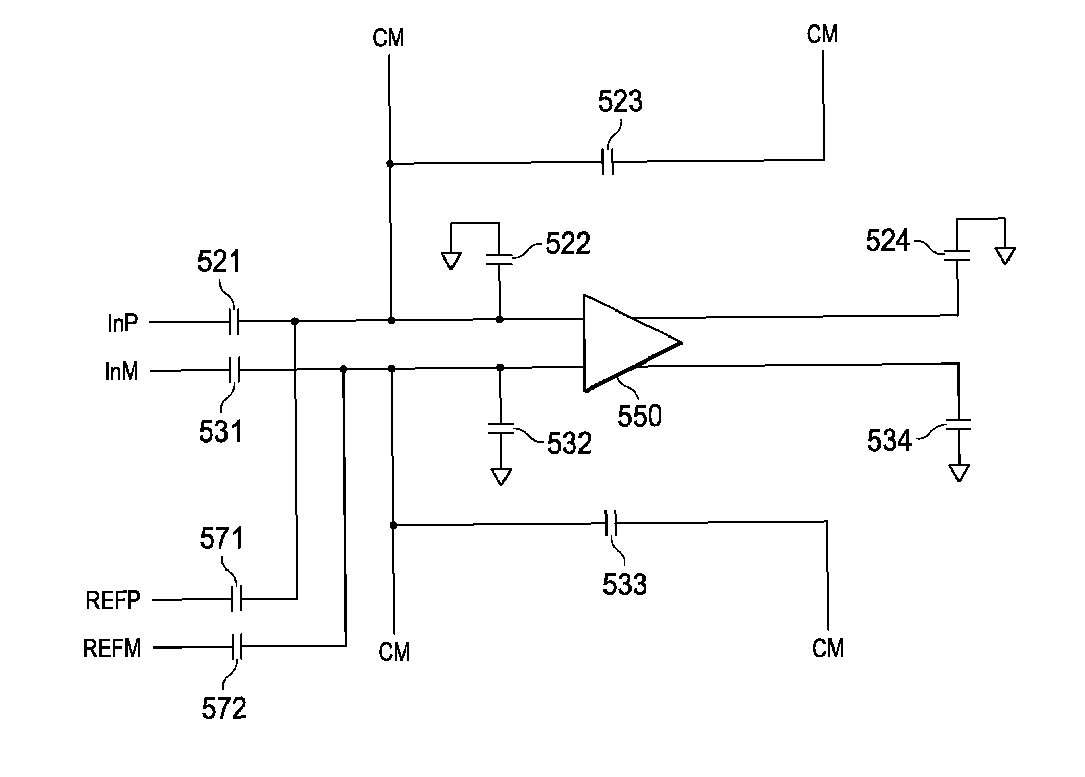
[0051]1. Overview

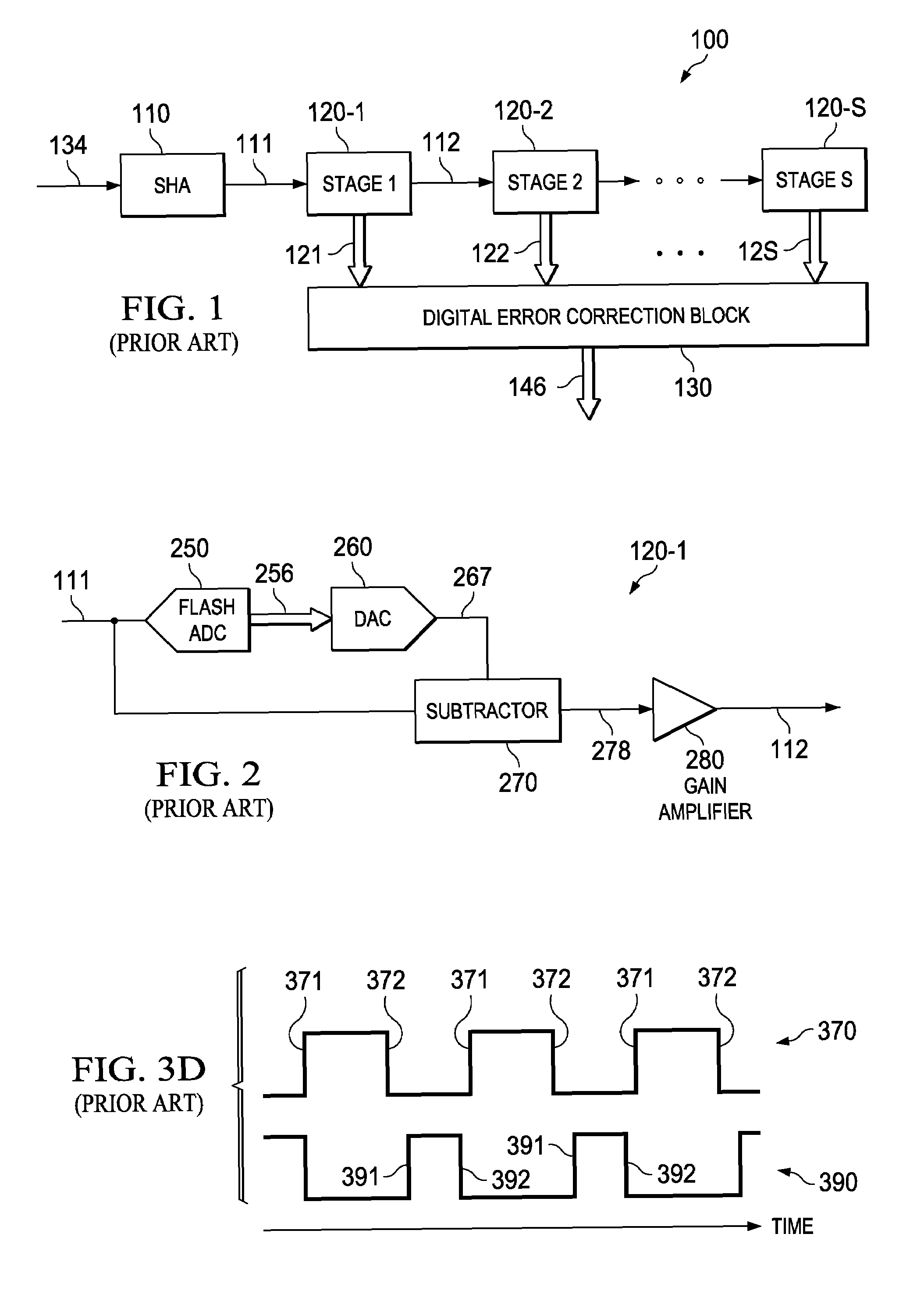
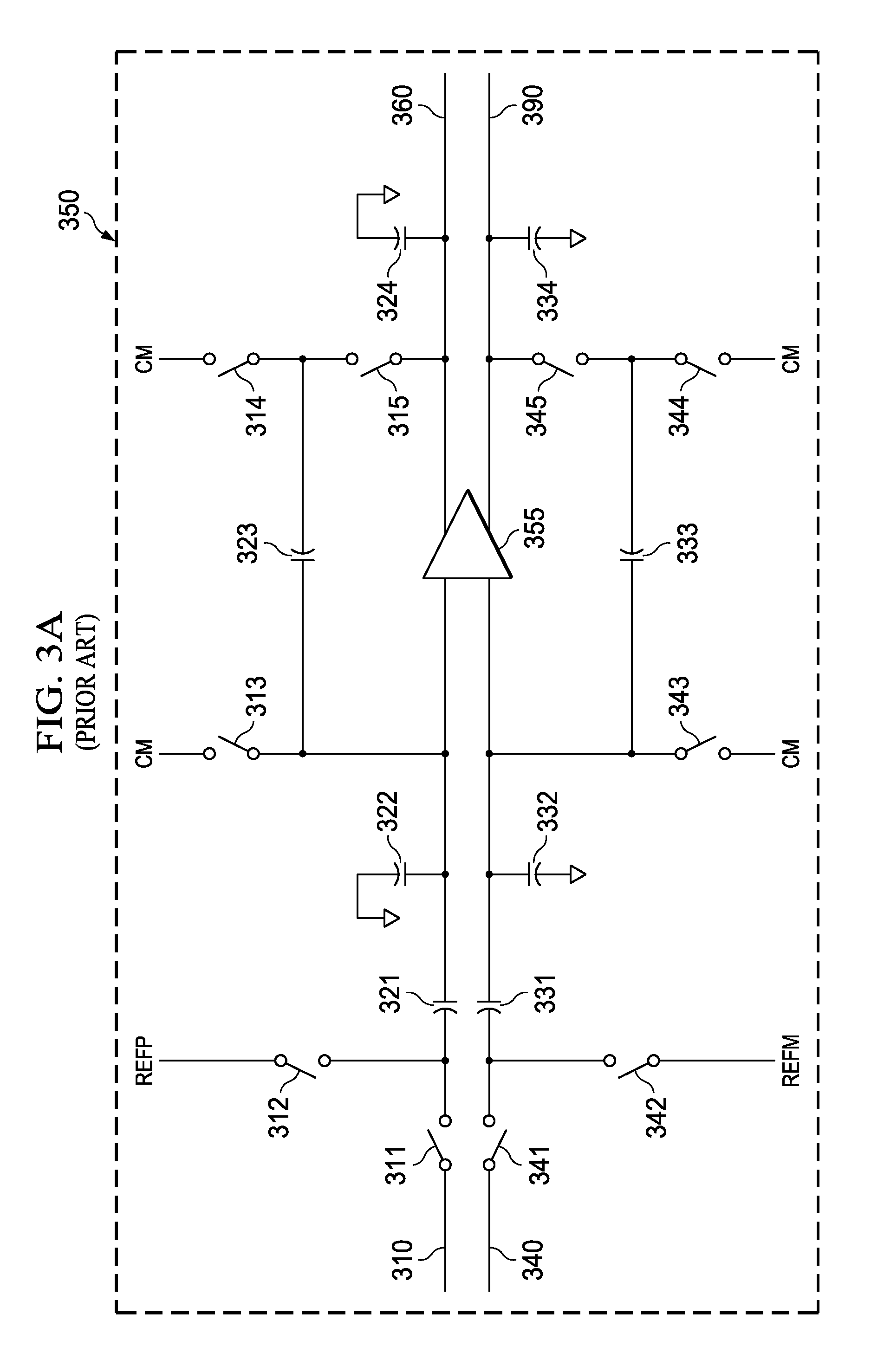
[0052]An aspect of the present invention ensures that (substantially) equal common mode voltage is present at the input terminals of an operational amplifier (amplifying the residue signal in a stage of an ADC in two phases) while reducing the noise introduced into the amplified signal. Such a feature is obtained by using a first reference capacitor which is coupled between an input terminal of the operational amplifier and a reference voltage in a first phase, and between the input terminal and the reference voltage but with opposite polarity in the second phase.

[0053]Several aspects of the invention are described below with reference to examples for illustration. It should be understood that numerous specific details, relationships, and methods are set forth to provide a full understanding of the invention. One skilled in the relevant art, however, will readily recognize that the invention can be practiced without one or more of the specific details, or with other...


PUM


Abstract

Equal common mode voltage is present at the input terminals of an operational amplifier with amplifies the residue signal in a stage of an ADC in two phases while reducing the noise introduced into the amplified signal. A reference capacitor is coupled between an input terminal of the operational amplifier and a reference voltage in a first phase, and between the input terminal and a the reference voltage but with opposite polarity in the second phase.

Description

RELATED APPLICATION [0001]The present application claims priority from the copending U.S. Provisional Patent Application entitled, “Technique to sample reference voltage to reduce thermal noise in switched capacitor amplifiers”, Ser. No. 60 / 601,900, filed Aug. 16, 2004, the entirety of whith is incorporated by reference herein.BACKGROUND [0002]1. Field of the Invention[0003]The present invention relates to integrated circuit design, and more specifically to a method and apparatus for reducing noise in a switched capacitor amplifier circuit sampling a reference voltage.[0004]2. Related Art[0005]Amplifier circuits (amplifiers) are often employed to amplify signals. In general, an amplifier amplifies an input signal and provides the amplified signal as an output signal. A switched capacitor amplifier is a type of amplifier circuit, which contains operational amplifier(s) (op-amp), switches and capacitors driven by clock signals. The switches are operated to control the connections and ...

Claims


Application Information

Patent Timeline
Patent Type & Authority Patents(United States)
IPC IPC(8): H03F1/02
CPCH03F1/02H03F1/26H03F3/005H03F3/45475H03F3/45973H03F2200/294
Inventor PERDOOR, SANDEEP MALLYAPENTAKOTA, VISVESVARAYA AAYYAGARI, RAVISHANKAR S
Owner TEXAS INSTR INC
Why Eureka
Try Eureka