Defect detection apparatus

a technology of defect detection and detection apparatus, which is applied in the direction of digital signal error detection/correction, instruments, recording signal processing, etc., can solve the problems of difficult to carry out accurate defect detection during a period, and the variable gain amplifier b>1000/b> cannot completely remove the level difference between the reflected light and the reflected light, so as to reduce the occurrence of false defect signals

Inactive Publication Date: 2008-04-22
PANASONIC CORP
View PDF3 Cites 2 Cited by
  • Summary
  • Abstract
  • Description
  • Claims
  • Application Information

AI Technical Summary

Benefits of technology

[0014]The present invention is made to solve the above-described problems and has for its object to provide a defect detection apparatus that can accurately and speedily detect a defect immediately after the operation of the optical disc drive has been switched between recording and playback.
[0024]As described above, in the defect detection apparatus according to the present invention, the output of the integration circuit is fixed to a reference voltage during a predetermined period after the operation of the optical disc drive has changed from playback to recording or from recording to playback, and the slice level that is set with reference to the output value is compared with the level of the envelope signal to output a defect detection signal. Therefore, the envelope signal is prevented from erroneously becoming lower than the slice level, thereby reducing occurrences of false defect signals during the above-mentioned period. Further, during a predetermined period after the above-mentioned period has ended, the envelope signal is integrated with the time constant of the integration circuit being reduced so that the change in the waveform of the output signal IS from the integration circuit quickly follows the change in the waveform of the envelope signal EM, whereby defect detection can be speedily restarted.

Problems solved by technology

However, since the gain set value of the variable gain amplifier 1000 has some degree of variation or the like, it is difficult for the variable gain amplifier 1000 to completely remove the level difference between the reflected light during recording of the reflection signal AS and the reflected light during playback thereof.
In the conventional defect detection apparatus, such level difference causes problems as follows.
Further, when the operation to the optical disc has changed from playback to recording, no false defect signal FS is output, but it is difficult to carry out accurate defect detection during a period tF in the defect detection signal DD shown in FIG. 10.

Method used


Image

  • Defect detection apparatus
  • Defect detection apparatus
  • Defect detection apparatus

Examples


embodiment 1

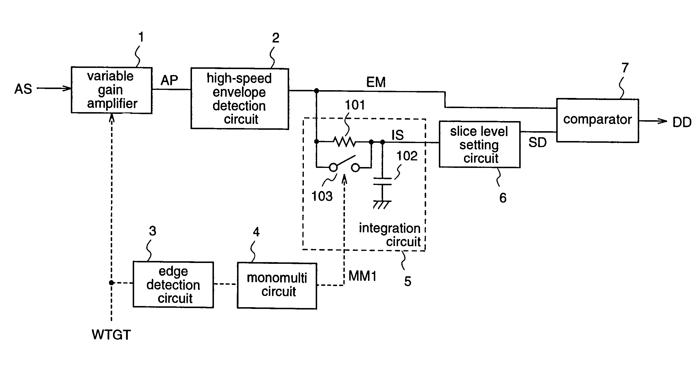
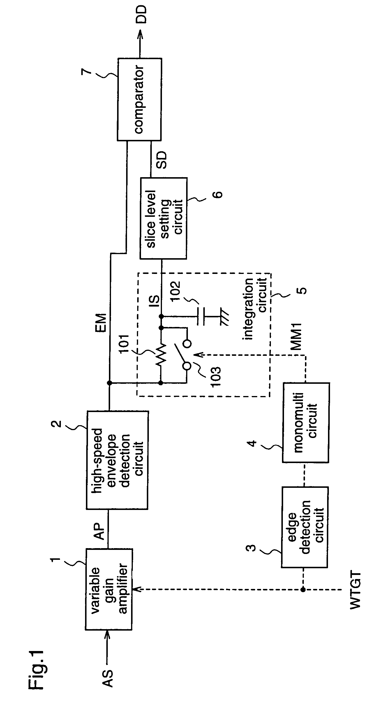
[0035]FIG. 1 is a block diagram illustrating the construction of a defect detection apparatus according to a first embodiment of the present invention.

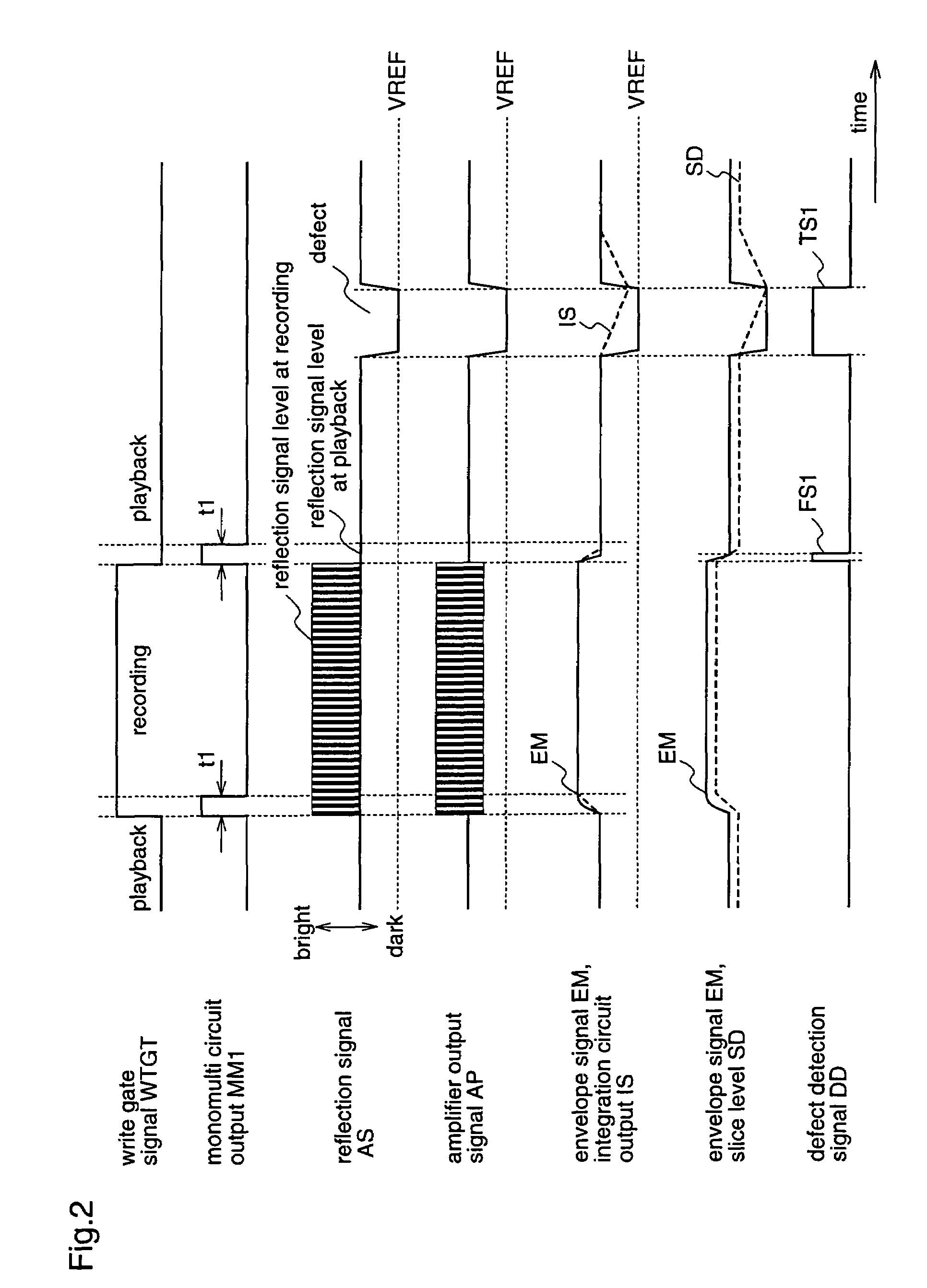
[0036]In FIG. 1, reference numeral 1 denotes a variable gain amplifier as an amplifier circuit for amplifying a reflection signal AS which is obtained according to the intensity of reflected light of a light beam applied onto an optical disc. The variable gain amplifier 1 is supplied with a write gate signal WTGT indicating whether the operation of an optical disc drive is recording or playback. Hereinafter, it is assumed that the write gate signal WTGT is “H” during recording onto the optical disc, and “L” during playback from the optical disc. Reference numeral 2 denotes a high-speed envelope detection circuit as an envelope detection circuit for detecting an envelope of an output signal AP of the variable gain amplifier 1. The high-speed envelope detection circuit 2 is a typical detector, and obtains an upper envelope of the output...

embodiment 2

[0047]FIG. 3 is a block diagram illustrating a defect detection apparatus according to a second embodiment of the present invention. In FIG. 3, a variable gain amplifier 10, a high-speed envelope detection circuit 11, an edge detection circuit 12, a monomulti circuit 13, an integration circuit 14, a slice level setting circuit 16, and a comparator 17 are identical to those of the defect detection apparatus according to the first embodiment, and therefore, repeated description is not necessary. In this second embodiment, a slice level switching circuit 15 instructs the slice level setting circuit 16 to set a slice level which is shifted toward a reference voltage VREF side relative to the normal slice level, during a period when the slice level switching circuit 15 receives the pulse signal MM1 outputted from the monomulti circuit 13.

[0048]Next, the operation of the defect detection apparatus constructed as described above will be described with reference to FIGS. 3 and 4. FIG. 4 sho...

embodiment 3

[0053]FIG. 5 is a block diagram illustrating the construction of a defect detection apparatus according to a third embodiment of the present invention.

[0054]In FIG. 3, a variable gain amplifier 20, a high-speed envelope detection circuit 21, an edge detection circuit 22, a slice level setting circuit 25, and a comparator 26 are identical to those of the defect detection apparatus according to the first embodiment, and therefore, repeated description is not necessary. In this third embodiment, reference numeral 24 denotes an integration circuit for integrating the envelope signal EM outputted from the high-speed envelope detection circuit 21. The integration circuit 24 is provided with a resistor 301, a capacitor 302, and a switch 303. An end of the resistor 301 is supplied with the envelope signal EM, and the other end is connected to the slice level setting circuit 25, the capacitor 302, and the switch 303. An end of the switch 303 is connected to the reference voltage VREF, and th...


PUM

PropertyMeasurementUnit
lengthaaaaaaaaaa
time constantaaaaaaaaaa
voltageaaaaaaaaaa

Abstract

During a predetermined period of time after the operation of an optical disc drive has changed from recording to playback or from playback to recording, a first monomulti circuit outputs a pulse signal according to the operation change of the optical disc drive. On receipt of the pulse signal, a capacitor included in an integration circuit is short-circuited at a predetermined reference voltage to fix the output value of the integration circuit at the reference voltage. After the period has passed, on receipt of a pulse signal outputted from a second monomulti circuit, a resistor included in the integration circuit is short-circuited, and an envelope signal is integrated with a time constant being reduced, whereby detection of a false defect signal is avoided, and defect detection can be speedily restarted.

Description

FIELD OF THE INVENTION[0001]The present invention relates to a defect detection apparatus which is used in an optical disc drive or the like and, more particularly, to a defect detection apparatus which accurately performs defect detection immediately after the operation of the optical disc drive has been changed from recording to playback or from playback to recording.BACKGROUND OF THE INVENTION[0002]In recent years, as the amount of information has significantly been increased in a computer system, a large-capacity, high-speed, and random-accessible optical disc drive has come into wide use as an information data recording / playback apparatus, and optical discs such as CD-R, CD-RW, DVD-R / RW, and DVD-RAM have been used as recording media.[0003]Such optical disc drive employs a defect detection apparatus for detecting a defect that is an area where writing or reading in / from the optical disc is not normally carried out. More specifically, when a light beam is converged and applied on...

Claims


Application Information

Patent Timeline
Patent Type & Authority Patents(United States)
IPC IPC(8): G11B7/00G11B5/09G11B7/004G11B20/10G11B7/09G11B19/02G11B20/18
CPCG11B20/10037G11B20/18G11B19/02
Inventor TORII, TOSHIHIROIZUMI, TERUHIKO
Owner PANASONIC CORP
Why Eureka
Try Eureka