Method and Apparatus for Inspecting Defects

a defect detection and defect technology, applied in the direction of material analysis through optical means, measurement devices, instruments, etc., can solve the problems of defect detection performance decline, and difficulty in high sensitivity detection of short-circuit defects at the bottom of patterns, so as to achieve high-precision defect detection

US20100014075A1Inactive Publication Date: 2010-01-21HITACHI HIGH-TECH CORP
4 Cites 7 Cited by

Patent Information

Authority / Receiving Office
US · United States
Patent Type
Applications(United States)
Current Assignee / Owner
Publication Date
2010-01-21
Estimated Expiration
Not applicable · inactive patent

Smart Images

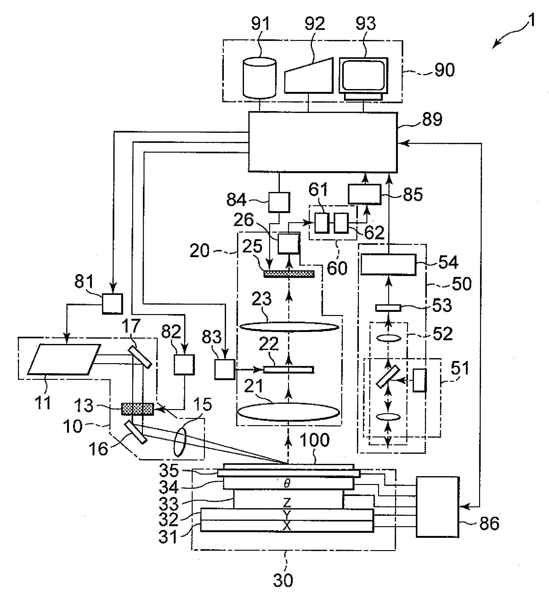
  • Figure 1
    Figure 1
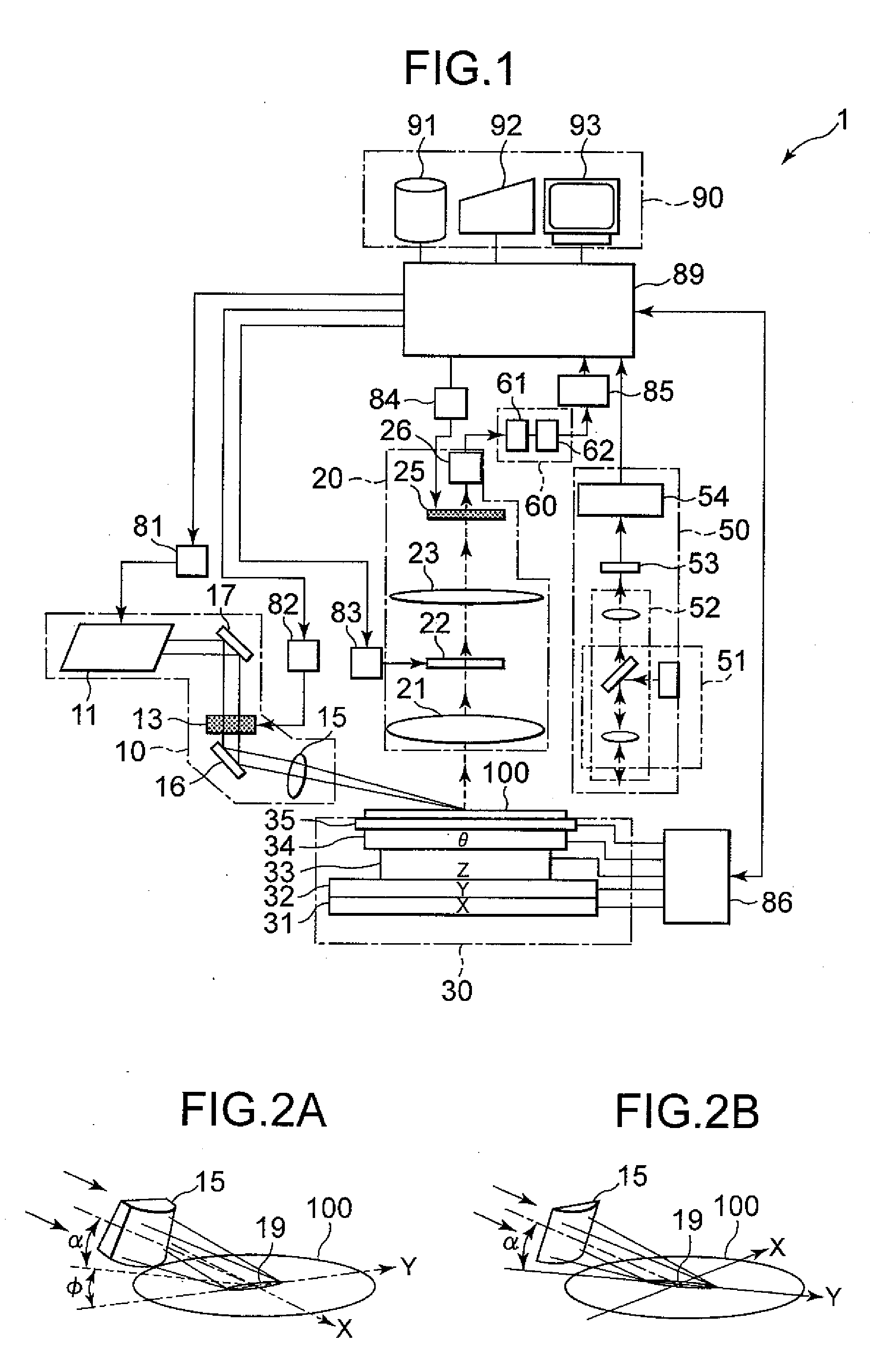
  • Figure 2
    Figure 2
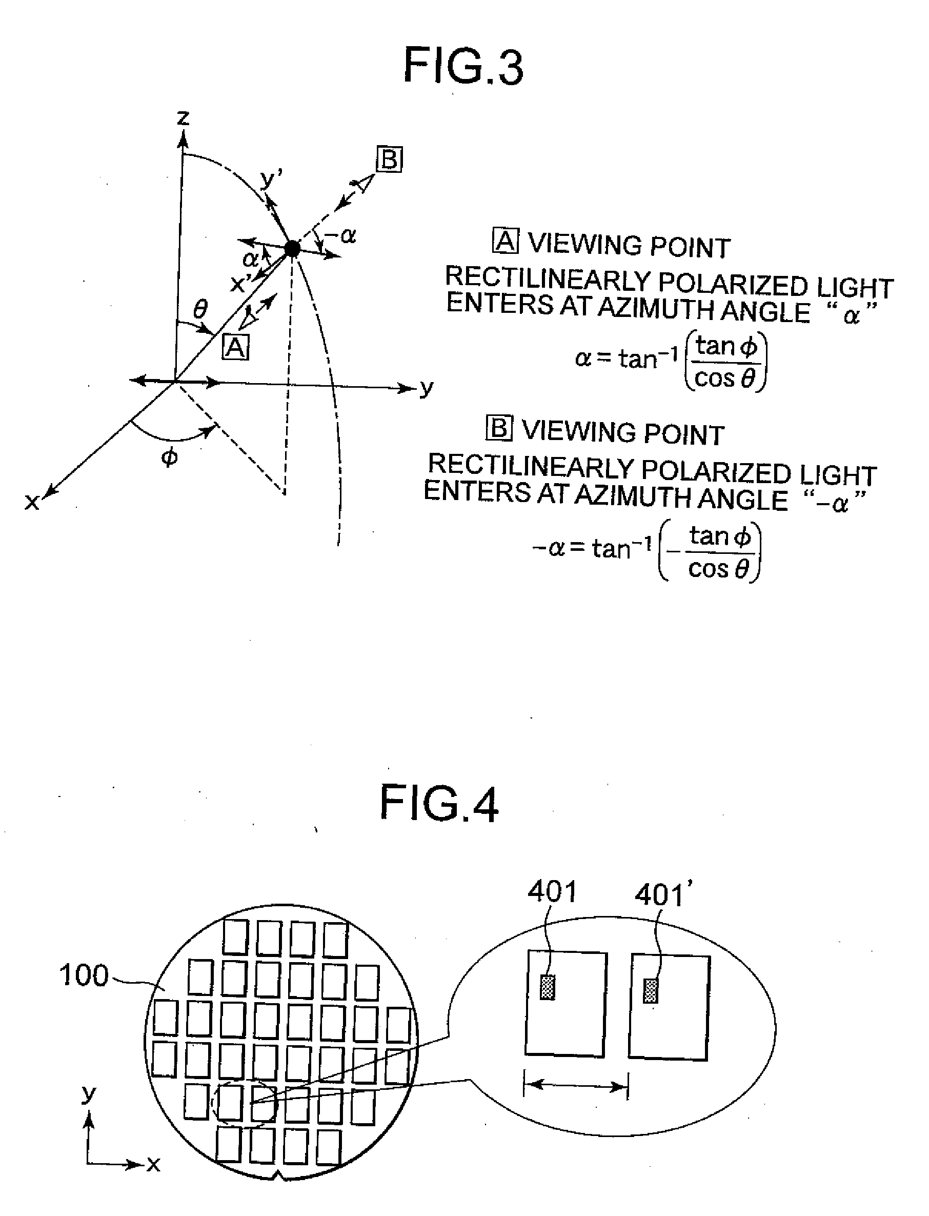
  • Figure 3
    Figure 3
Patent Text Reader

Abstract

An apparatus for inspecting a substrate surface is provided, which includes illumination optics for irradiating the substrate surface linearly with rectilinearly polarized light from an oblique direction, detection optics for acquiring images of the substrate surface, each of the images being formed by the light scattered from the light-irradiated substrate surface, and means for comparing an image selected as an inspection image from the plurality of substrate surface images that the detection optics has acquired to detect defects, and another image selected from the plural images of the substrate surface as a reference image different from the inspection image; the illumination optics being formed with polarization control means for controlling a polarizing direction of the light according to a particular scanning direction of the substrate or a direction orthogonal to the scanning direction.
Need to check novelty before this filing date? Find Prior Art

Description

BACKGROUND OF THE INVENTION

[0001] The present invention relates generally to defect inspection methods and apparatus for detecting microstructured pattern defects, contamination, and the like, by comparing an optically acquired image of an object to be inspected, and a reference image. More particularly, the invention relates to a method and apparatus for inspecting defects in a semiconductor device, a photomask, a liquid crystal, and other objects, in optical technique.

[0002] During the manufacture of a semiconductor device, a substrate (wafer) on which the semiconductor device is to be formed undergoes processing through hundreds of manufacturing process steps to become a product. In these process steps, for example, if any kinds of contamination sticking to the surface of the substrate (wafer) are found or if the nonuniformity of pattern formation between processes occurs, these undesirable events will cause pattern defects, rendering the semiconductor device defective. In addition...

Examples

second embodiment

[0099]A second embodiment of an inspection apparatus according to the present invention is described below with reference to FIG. 15, a block diagram of the inspection apparatus. In the description below, the same constituent elements as those of the first embodiment are omitted and focus is placed primarily upon differences. The inspection apparatus 1 includes, as appropriate, first illumination optics 10, second illumination optics 1510, detection optics 20, a substrate conveying circuit 30, a focal measuring circuit 50 (not shown), an image-processing circuit 60, a control and processing circuit, and an interface circuit 90.

[0100]The first illumination optics 10 is constructed using, as appropriate, a laser light source 11, reflecting mirrors 16 and 17 that guide in a required direction the light emitted from the laser light source 11, a polarization control unit 13, a condensing lens 15, and an optical splitting element 1501 provided between the reflecting mirror 17 and the pola...