Image sensing device

a sensing device and image technology, applied in the field of image sensing devices, can solve the problems of signal saturation, defective pixel always becomes a black dot, and the detected signal is saturated, and achieve the effect of correct detection of defective pixel

a sensing device and image technology, applied in the field of image sensing devices, can solve the problems of signal saturation, defective pixel always becomes a black dot, and the detected signal is saturated, and achieve the effect of correct detection of defective pixel

US20100025568A1Inactive Publication Date: 2010-02-04PIONEER CORP +3

Image

  • Image sensing device
  • Image sensing device
  • Image sensing device

Examples


Embodiment Construction

[0022]The embodiments of the present invention will now be described with reference to the drawings.

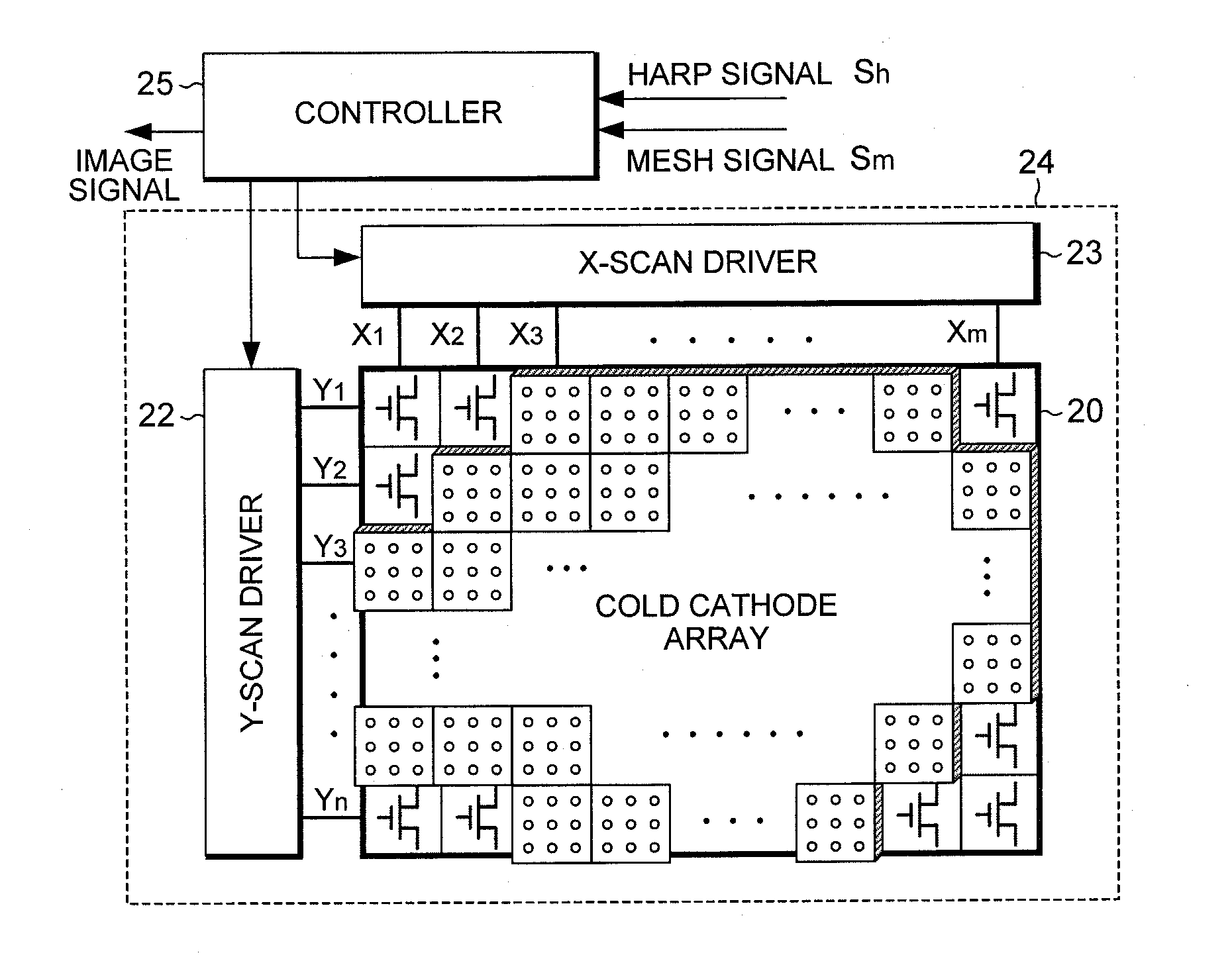
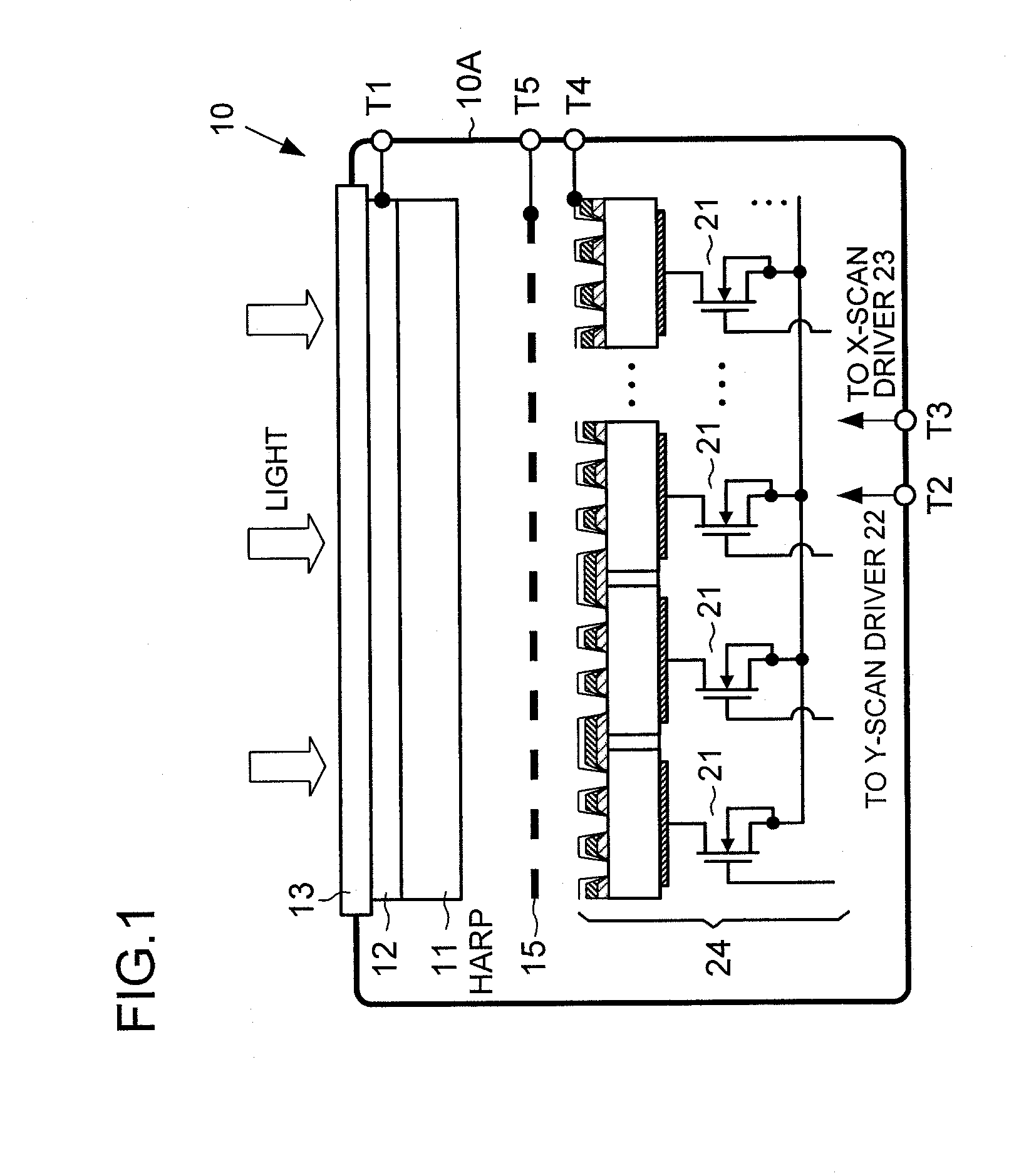
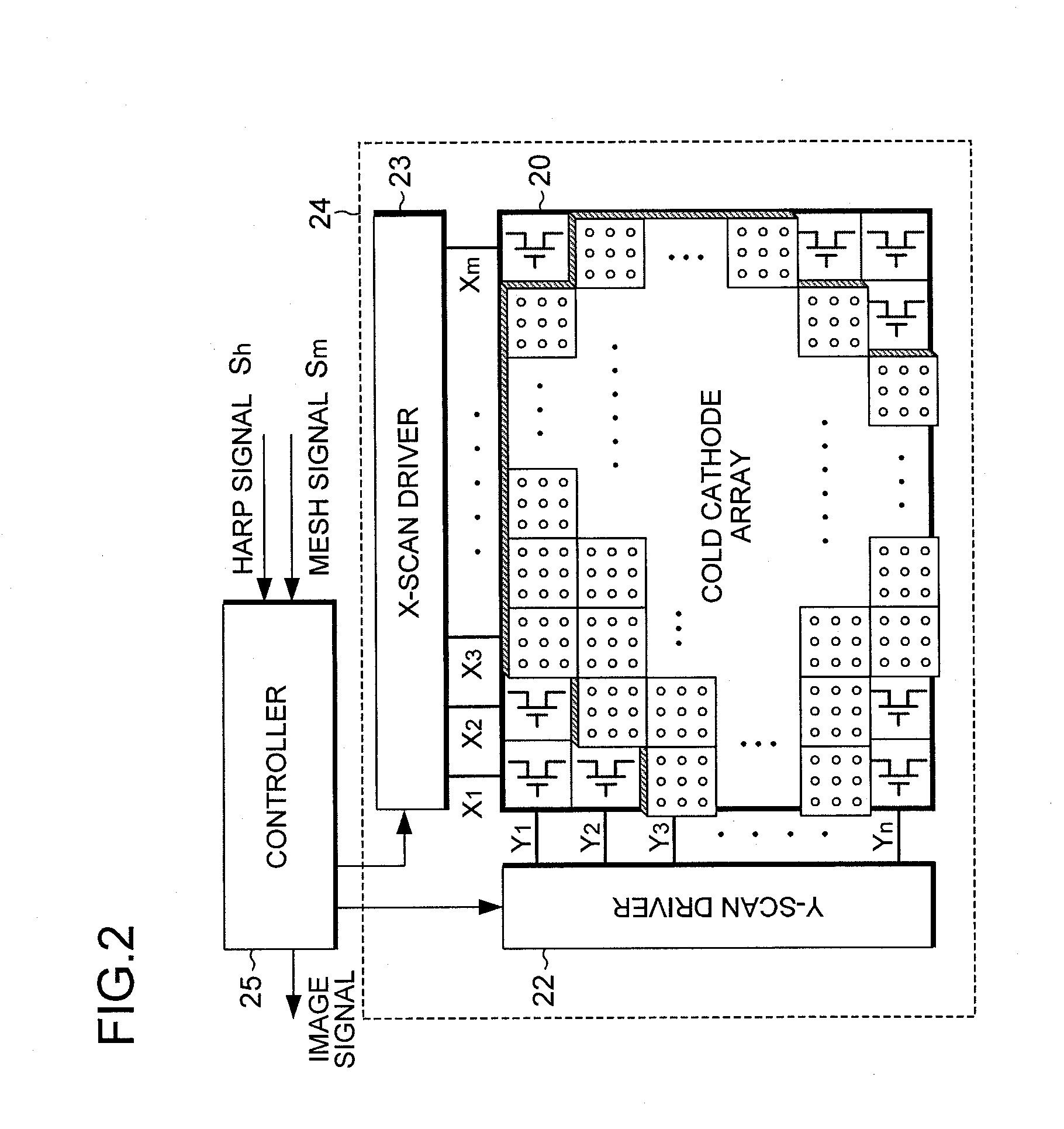
[0023]FIG. 1 is a cross-sectional view schematically illustrating a configuration of an HEED cold cathode HARP image sensor 10. The HEED cold cathode HARP image sensor 10, which will hereinafter also be referred to as a “cold cathode image sensor” for short, is an image sensor which combines a High-efficiency Electron Emission Device (HEED) with a High-gain Avalanche Rushing amorphous Photoconductor (HARP). In more detail, the cold cathode image sensor 10 includes an HARP photoelectric conversion film 11, an HEED cold cathode array chip 24, and a mesh electrode (intermediate electrode) 15 which is disposed between the HARP photoelectric conversion film 11 and the HEED cold cathode array 20. As described later, the HEED cold cathode array chip 24 integrally includes an active-matrix HEED cold cathode array 20, which will hereinafter be referred to as an “HEED cold cathode array” for sh...


PUM


Abstract

A device includes an electron emission source array including a plurality of electron emission sources, a photoelectric conversion film disposed to face the electron emission source array, and an intermediate electrode provided between the electron emission source array and the photoelectric conversion film, and an intermediate electrode current detector that applies a positive potential, relative to a potential of the electron emission source array, to the intermediate electrode and detects a current flowing in the intermediate electrode.

Description

BACKGROUND OF THE INVENTION[0001]1. Field of the Invention[0002]The present invention relates to an image sensing device that includes an image sensor having both an array of electron emission sources and a photoelectric conversion film and a drive circuit that drives the image sensor.[0003]2. Description of the Related Art[0004]An image sensing device, which includes an image sensor having an array of electron emission sources arranged in a matrix, each outputting electrons through application of an electric field, and a photoelectric conversion film, has been proposed. For example, a High-efficiency Electron Emission Device (HEED) has been proposed as an electron emission source (specifically, as a cold cathode electron source) (for example, see Pioneer R&D, Vol. 17, No. 2, 2007, pp. 61-69).[0005]The HEED enables low-voltage driving and features a simple structure, and studies are underway on application of HEEDs to image sensing devices. An example of the photoelectric conversion...

Claims


Application Information

Patent Timeline
04 Feb 2010
Publication
US20100025568A1
IPC
H01L31/02; H04N25/00
CPC
H01L27/14609; H01L27/14632; H04N5/374; H04N5/367; H01L31/107; H04N25/68; H04N25/76
Inventors
OKUDA, YOSHIYUKI; NANBA, MASAKAZU