[0010]The present invention was made in consideration of the above-described problems in known technologies. Accordingly, it is an object of the present invention to provide a microswitch capable of efficiently switching high-frequency signals at a low power consumption and having excellent responsiveness, excellent durability, and high reliability of long term driving, as well as a method for manufacturing the same.
[0025][13] A method for manufacturing a microswitch provided with a movable electrode contact component including a bending displacement component and a movable electrode, the bending displacement component having a thin plate and at least one support portion joined to an end portion of the above-described thin plate; a bending displacement mechanism disposed on at least one surface of the above-described thin plate and having a film piezoelectric / electrostrictor and at least one pair of voltage application electrode layers; and a wiring board joined to the above-described support portion of the above-described movable electrode contact component and having a signal line electrode layer disposed on the surface thereof, the signal line electrode layer facing the above-described movable electrode, the method including the steps of stacking and firing a plurality of ceramic green sheets in a predetermined shape to produce a ceramic structure, in a first step; integrally-forming the above-described bending displacement mechanism on a predetermined surface of the above-described ceramic structure by firing to produce a bending displacement mechanism unit, in a second step; mounting the above-described movable electrode at a predetermined position to produce a movable electrode unit, in a third step; forming the above-described signal line electrode layer on an insulating substrate to prepare the above-described wiring board, in a fourth step; and mounting the above-described movable electrode unit on the above-described wiring board and eliminating unnecessary portions to produce at least one microswitch, in a fifth step; and
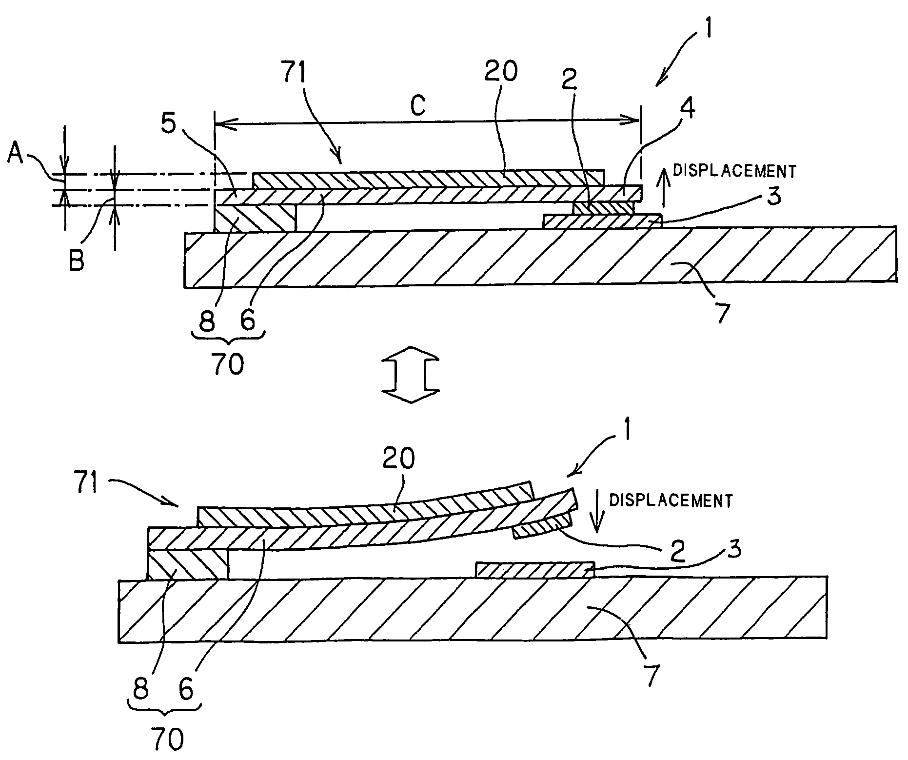
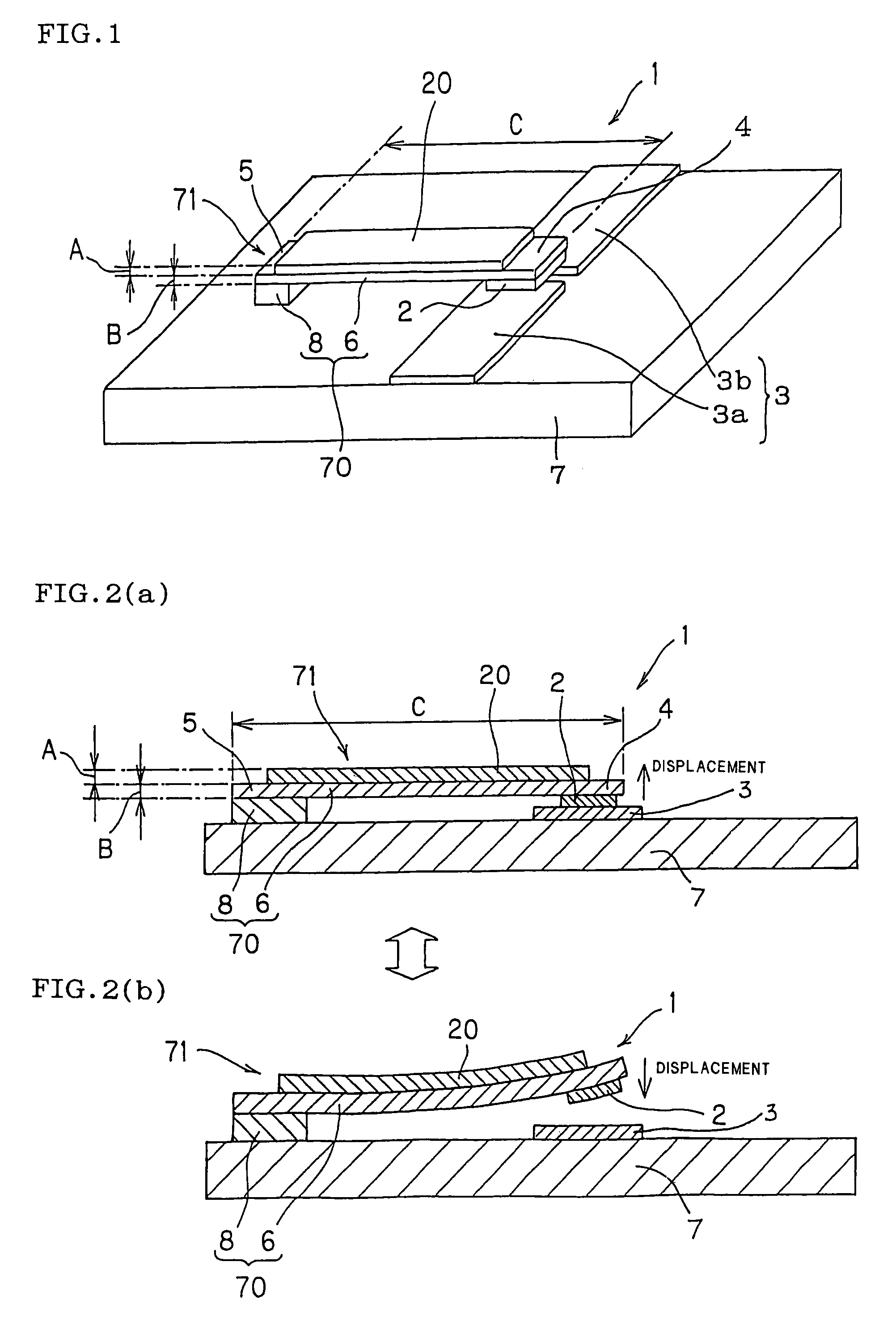
[0027]The first microswitch of the present invention is provided with a movable electrode contact component including a bending displacement component and a movable electrode, the bending displacement component having a thin plate and at least one support portion joined to an end portion of the thin plate; a bending displacement mechanism disposed on at least one surface of the thin plate and having a film piezoelectric / electrostrictor and at least one pair of voltage application electrode layers; and a substrate joined to the above-described support portion of the movable electrode contact component and having a fixed electrode disposed on the surface thereof, the fixed electrode facing the movable electrode, wherein the bending displacement mechanism is driven to displace the movable electrode, so that the movable electrode and the fixed electrode can be brought into a state of being electrically connected to each other or disconnected from each other, at least the thin plate of the bending displacement component is made of a ceramic material, and the thin plate, the piezoelectric / electrostrictor, and the voltage application electrode layers are integrated by firing. Therefore, effects are exerted on that switching of high-frequency signals can be performed efficiently at a low power consumption and that excellent responsiveness, excellent durability, and high reliability of long term driving are exhibited.
[0028]The second microswitch of the present invention is provided with a movable electrode component including a bending displacement component composed of a thin plate and a movable electrode; a bending displacement mechanism disposed on at least one surface of the thin plate and having a film piezoelectric / electrostrictor and at least one pair of voltage application electrode layers; and a substrate joined to one end portion of the thin plate of the movable electrode component and having a fixed electrode disposed on the surface thereof, the fixed electrode facing the movable electrode, wherein the bending displacement mechanism is driven to displace the movable electrode, so that the movable electrode and the fixed electrode can be brought into a state of being electrically connected to each other or disconnected from each other, at least the thin plate of the bending displacement component is made of a ceramic material, and the thin plate, the piezoelectric / electrostrictor, and the voltage application electrode layers are integrated by firing. Therefore, effects are exerted on that switching of high-frequency signals can be performed efficiently at a low power consumption and that excellent responsiveness, excellent durability, and high reliability of long term driving are exhibited. Preferably, the fixed electrode and the movable electrode are constructed as signal line conductors and, thereby, a split wiring type switch having a configuration including a signal line can be produced. Consequently, the switch can be made more compact and has excellent mountability.
[0029]The third microswitch of the present invention is provided with a movable electrode contact component including a bending displacement component and one pair of movable electrodes, the bending displacement component having one pair of thin plates disposed facing each other and a support portion joining one end portion of each of the thin plates to each other; and a bending displacement mechanism disposed on at least one surface of each of the thin plates and having a film piezoelectric / electrostrictor and at least one pair of voltage application electrode layers, wherein the bending displacement mechanism is driven to displace the movable electrodes, so that the movable electrodes can be brought into a state of being electrically connected to each other or disconnected from each other, at least the thin plate of the bending displacement component is made of a ceramic material, and the thin plate, the piezoelectric / electrostrictor, and the voltage application electrode layers are integrated by firing. Therefore, effects are exerted on that switching of high-frequency signals can be performed efficiently at a low power consumption and that excellent responsiveness, excellent durability, and high reliability of long term driving are exhibited.
[0030]According to the method for manufacturing a microswitch of the present invention, the microswitch of the present invention capable of efficiently switching high-frequency signals at a low power consumption and having excellent responsiveness, excellent durability, and high reliability of long term driving can be efficiently and simply produced.

