Dielectric resonator, dielectric resonator frequency adjusting method, and dielectric resonator integrated circuit

a dielectric resonator and frequency adjusting technology, applied in the direction of resonators, oscillating generators, semiconductor devices, etc., can solve the problem of large circuit siz

Active Publication Date: 2008-05-27
NEC CORP
View PDF6 Cites 11 Cited by
  • Summary
  • Abstract
  • Description
  • Claims
  • Application Information

AI Technical Summary

Problems solved by technology

That is, the lines and the transistor FET can not be disposed in upward and bottomward of the resonator, thereby resulting in large size of the circuit.

Method used


Image

  • Dielectric resonator, dielectric resonator frequency adjusting method, and dielectric resonator integrated circuit
  • Dielectric resonator, dielectric resonator frequency adjusting method, and dielectric resonator integrated circuit
  • Dielectric resonator, dielectric resonator frequency adjusting method, and dielectric resonator integrated circuit

Examples


first embodiment

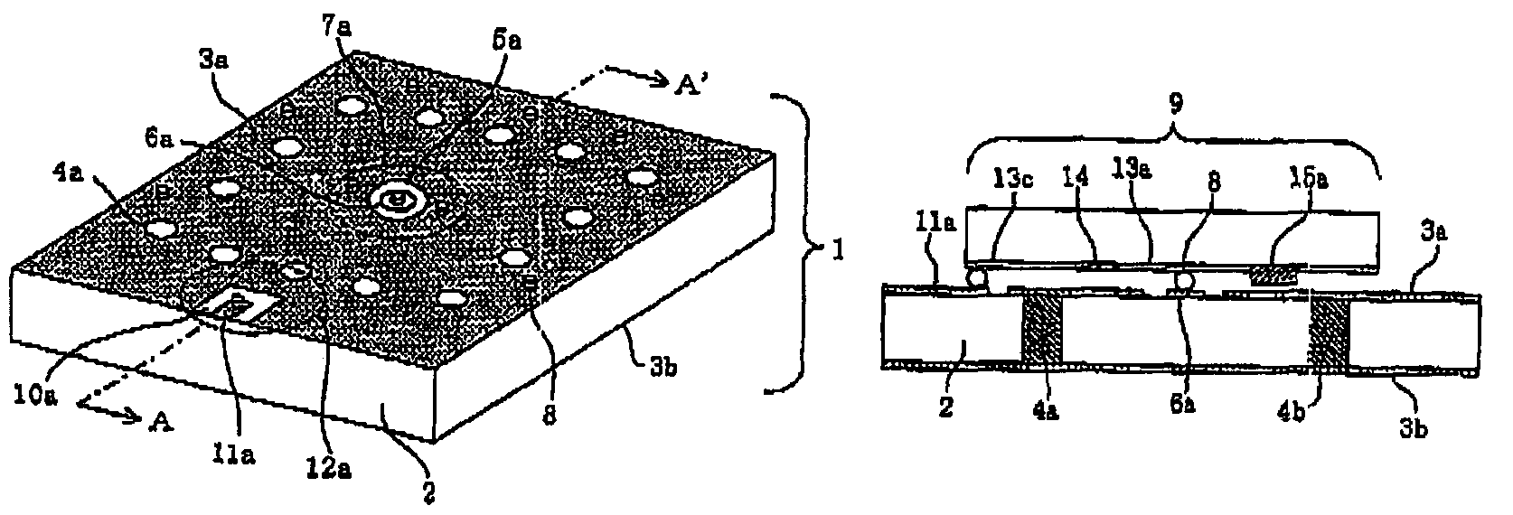
[0072]FIG. 3A is a perspective view showing a dielectric resonator in a first configuration example of a first embodiment of the present invention. FIG. 3B is a traverse cross sectional view at A-A′ dashed line in FIG. 3A showing an oscillator (DRO) having a dielectric resonator. FIG. 3C is an equivalent circuit of an oscillator (DRO) having a dielectric resonator shown in FIG. 3A. Dielectric resonator 1 is configured such that ground conductive layers 3a, 3b are formed on both sides of dielectric substrate 2, and the both conductive layers are connected with plug conductor 4b filling circularly-arranged via hole 4a. It is favorable that a distance between via holes 4a is less than ½, more favorably less than ¼ of a wave length in the dielectric substrate for suppressing leakage of the wave from a clearance between the via holes. A region surrounded by the via holes and ground conductive layers 3a, 3b is named an effective resonant region. In this configuration, dielectric resonator...

second embodiment

[0077]FIG. 6A is a plane view showing a dielectric resonator of a first configuration example in a second embodiment according to the present invention. FIG. 6B is an equivalent circuit of an oscillator (DRO) having the dielectric resonator shown in FIG. 6A. As the second embodiment, a configuration capable of electrically tuning a frequency of the oscillator (DRO) having the dielectric resonator will be shown. Two coupling elements 7d, 7e are formed on ground conductive layer 3a. Coupling element 7d is connected to transmission line 13a extending from a gate of transistor FET 14, and coupling element 7e is connected to varactor diode 20 formed on oscillation circuit MMIC 9. For applying control voltage 17c to varactor diode 20, coupling element 7e is DC connected to the ground through resistor 15c having several −kO. In addition, capacitor 21a which has a low reactance at an operating frequency is connected to the opposite side of coupling element 7e. By varying control voltage 17c...

third embodiment

[0078]FIG. 7A is a plane view showing a dielectric resonator of a first configuration example of a third embodiment according to the present invention. FIG. 7B is an equivalent circuit of an oscillator (DRO) having the dielectric resonator shown in FIG. 7A. An output of oscillation circuit 9 is connected to coupling element 7f, which is configured by forming slot 5d in ground conductive layer 3a, through capacitor 21b having a low reactance at an operating frequency which cuts DC bias. In addition, coupling element 7g is disposed in ground conductive layer 3a by forming slot 5e. Coupling element 7g is connected to coplanar line 12b consisting of ground conductive layer 3a formed to sandwich slot 10b with signal conductive layer 11b by stepping over the inside and the outside of the resonator. In this configuration, dielectric resonator 1 only outputs a resonant frequency, and reflects all waves other than the resonant frequency. In a configuration of this embodiment, a configuration...


PUM


Abstract

An oscillator comprising a dielectric resonator (DR) has a high controllability and reproducibility of coupling between the dielectric resonator (DR) and an oscillation circuit, and an integrated circuit is reduced in size. The dielectric resonator (DR) (1) is composed of a dielectric substrate (2), grounding conductive layers (3a, 3b) formed on both sides of the dielectric substrate (2), and via holes (4a) for electrical connection between the conductive layers. A coupling element (7a) composed of a slot (5a) provided in the central portion of the grounding conductive layer (3a) and a patch (6a) surrounded by the slot (5a) is coupled to the dielectric resonator (DR) (1). The patch (6a) is connected to a transmission line (13a) on an oscillation circuit (9) through a bump (8). The transmission line (13a) is connected to the ground through a termination resistor (15a). On the oscillation circuit MMIC (9), the transmission line (13a) is connected to the gate of a transistor FET (14) A capacitive transmission line (13a) for positive feedback is connected to the transistor FET (14). The output of the transistor FET (14) is connected to a transmission line (13c) for output through a matching circuit (16). The transmission line (13c) is bump-connected to a coplanar line (12a) composed of a signal conductive layer (11a) formed on an edge of the dielectric resonator (DR) (1) and the grounding conductive layer (3a).

Description

FIELD OF THE INVENTION[0001]The present invention relates to a dielectric resonator which is used in a microwave band and in a millimeter wave band, a frequency adjustment method for the waves of the bands, and an integrated circuit using the dielectric resonator.BACKGROUND OF THE INVENTION[0002]All of patents, patent applications, patent publications, scientific articles and the like, which will hereinafter be cited or identified in the present application, will hereby be incorporated by references in their entirety in order to describe more fully the state of the art, to which the present invention pertains.[0003]A dielectric resonator (DR) is used in an oscillator used in a microwave band and in a millimeter wave band for increasing stabilities for a phase noise and the frequency. FIG. 1 is an equivalent circuit showing a configuration of the oscillator using the dielectric resonator (DRO) according to one conventional example. For obtaining a negative resistance, a capacitive mi...

Claims


Application Information

Patent Timeline
Patent Type & Authority Patents(United States)
IPC IPC(8): H01P7/10H01P7/00H03B5/18
CPCH01P7/00H01P7/10H03B5/1876H01L2224/0554H01L2224/05568H01L2224/05573H01L2224/16227H01L2924/00014H01L2224/05599H01L2224/0555H01L2224/0556
Inventor ITO, MASAHARUMARUHASHI, KENICHIKISHIMOTO, SHUYAOHATA, KEIICHI
Owner NEC CORP
Why Eureka
Try Eureka