Switch element

a technology of switch element and contact element, applied in the field of switch element, can solve problems such as failure of switching function, and achieve the effect of exemplifying the performance of the contact elemen

Inactive Publication Date: 2008-06-03
SJOSTROM PHILIP ADRIAN
View PDF12 Cites 19 Cited by
  • Summary
  • Abstract
  • Description
  • Claims
  • Application Information

AI Technical Summary

Benefits of technology

[0014]The contact element may be provided with at least one or more formed contact points close to the centre of the dome which would reduce dome travel to prevent over extension of the dome and improve contact characteristics between the dome and pads or tracks on the printed circuit board or other substrate with conductive tracks. The device may be connected to external electrical or electronic circuits via conductive tracks on both or one side of the printed circuit substrate, which may feature conductive, plated-through holes to connect tracks from one side to the other.
[0030]Installation without the necessity of using a spacer may give a cheaper assembly.
[0031]The bearer element provides an optimised bed for the contact element, providing consistent, stable, and secure, long-life properties which can exemplify the performance of the contact element.

Problems solved by technology

First, the central portion of the domed element, in its relaxed or un-actuated state, is raised above the plane of the element's rim, ensuring that the central portion is poised above, yet electrically isolated from, a contact surface below the dome. This contact surface is generally provided on some type of printed circuit board which acts as a substrate upon which the dome is positioned to form an electrical switch. The clearance between these two elements is generally about one or two millimetres. The rim of the dome, when not actuated by a force which would distort its shape, is the only part of the unit which is in contact with an associated substrate, such as a PCB. Upon such a PCB is a conductive pad, generally in the form of a full or partial annular ring, upon which the dome's rim sits, being electrically in contact with it. This rim-contact pad is electrically isolated from a centralised contact pad which forms the second node of a simple switch, with the contacting element being the dome itself.
Second, the shape of the dome and the springy nature of the sheet material from which it is formed means that, when the dome's central portion is depressed (by a finger), it can be caused to deform in a sudden or “snap” action. The element, partly “flattened” in this way, can be made to electrically connect the inner and outer contact-pads upon a substrate such as a PCB. As this actuating pressure is steadily released, the domed element, due to the effects of its mechanical hysteresis will delay its return to its normal, un-actuated state, until it suddenly releases with a “snap-action”. This snap-action serves the very important function of providing tactile feedback to a human operator of the key-panel switch, ie; it signals to the operator the impression that a switching action has indeed occurred. This hysteresis also serves as a contact de-bounce mechanism, although this is not crucial these days because micro-controller programs, as commonly seen in situations using dome-switch key-pad fabrications, can easily ignore the effects of contact-bounce.
These dome can have problems of migration especially when used in a vertical position and the edges of the dome can wear away the conductive track on the PCB and so cause failure of the switching function.

Method used


Image

  • Switch element
  • Switch element
  • Switch element

Examples


Embodiment Construction

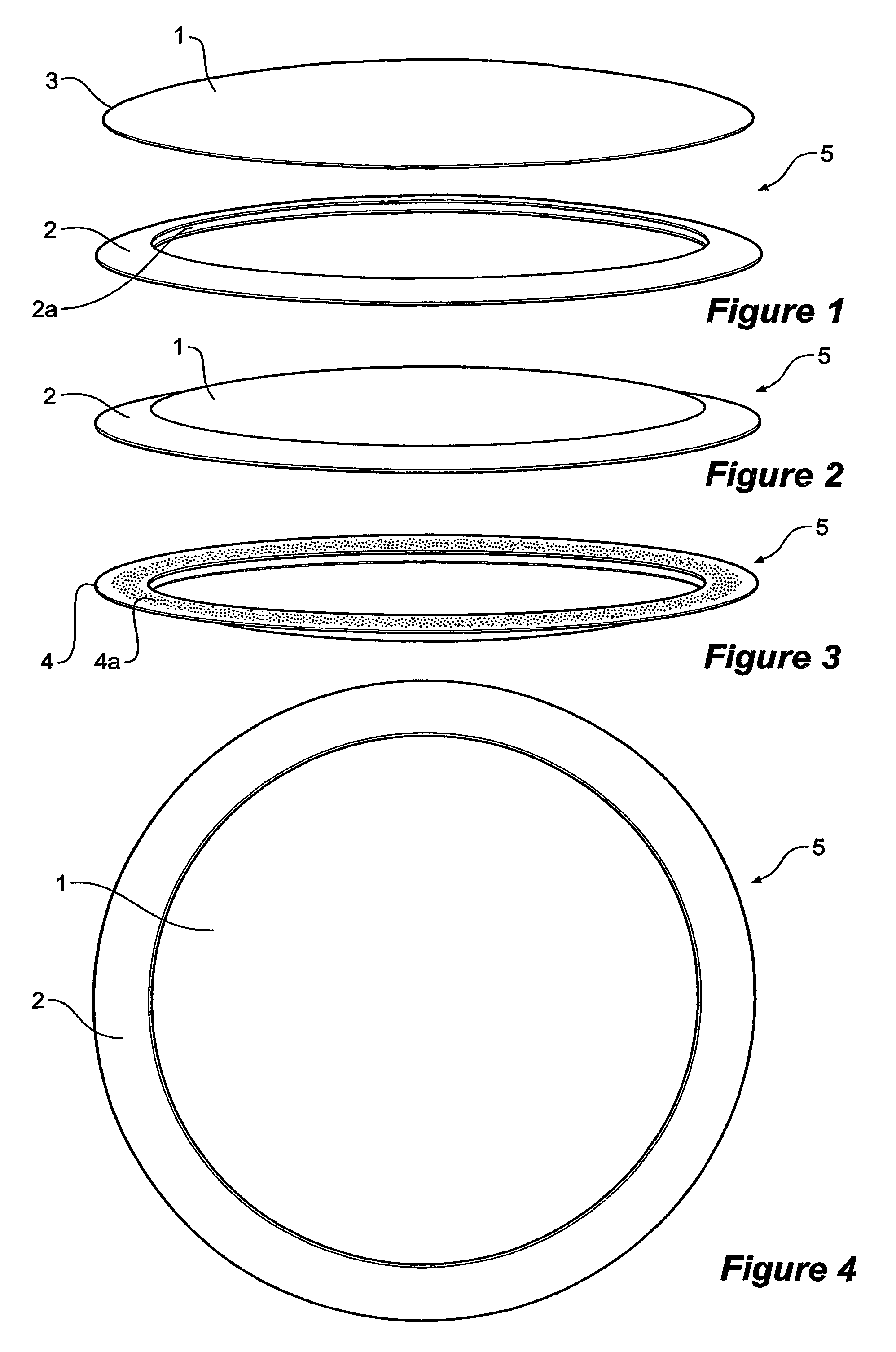
[0062]FIG. 1 shows an exploded perspective view of a contact element 1 and an associated bearer element 2 of a switch element 5. In this example, the contact element 1 is a diaphragm in the form of a shallow metal dome.

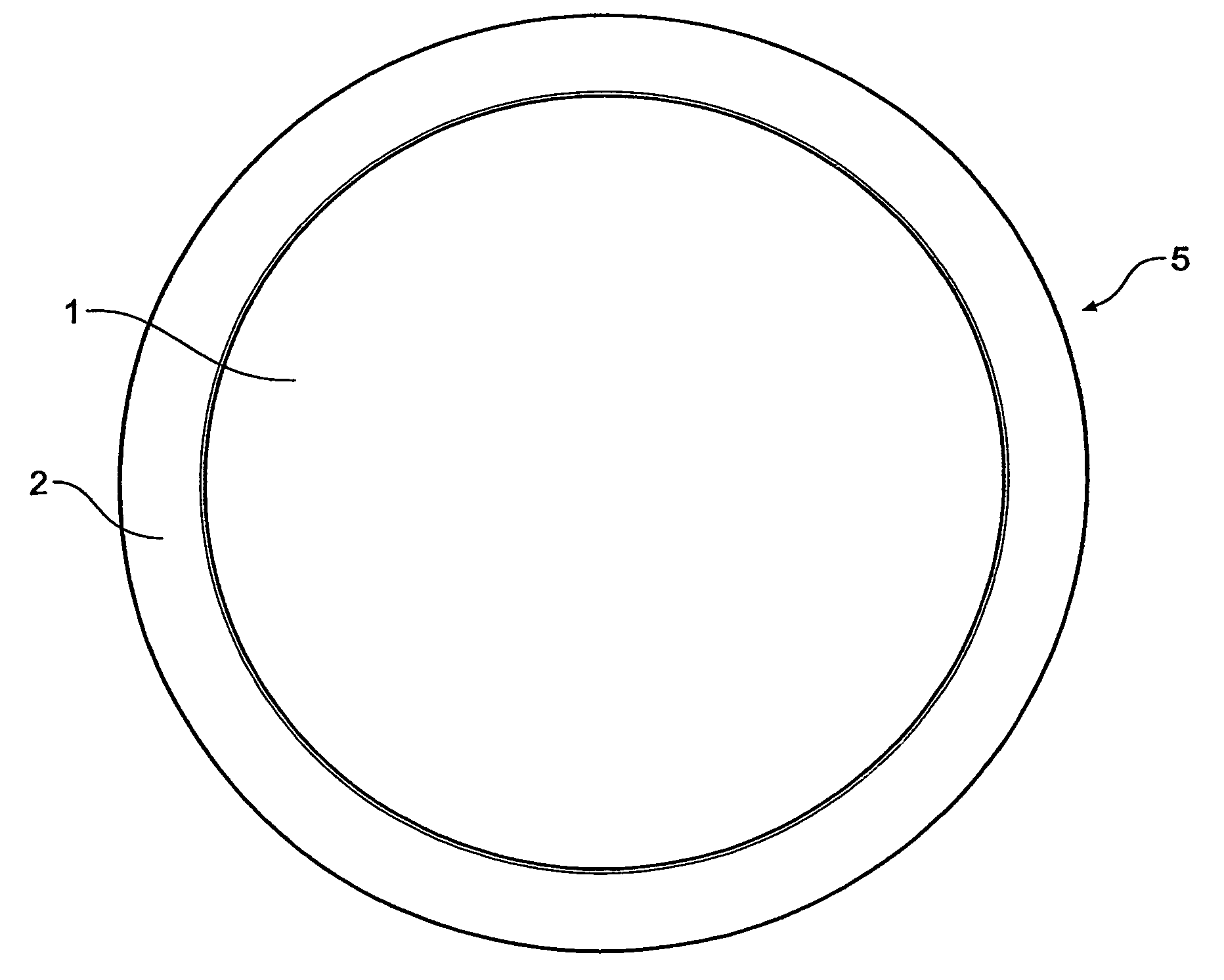
[0063]FIG. 2 shows the switch element 5 with the contact element 1 retained within the bearer element 2. The switch element, once assembled together, forms a unit, the parts of which are expected to be inseparable in all ordinary circumstances of application and operation. The diameter of the contact element is such that its rim 3 (see FIG. 1) will be held captive by the curved lip and so-formed inner surfaces of the bearer element which is in a C shape facing with its open side toward the centre of the bearer element. The rim of the diaphragm rests upon the hard inner surface of the bearer element, or may be additionally, lightly constrained by the internal “crease” formed by the retaining lip. The dimensions and profile of the diaphragm can be such that, in its un-a...


PUM


Abstract

A switch element for surface mounting onto a printed circuit board which has a bearer element (2) and a contact element (1). Both the bearer element and the contact element are formed from an electrically conductive material and the contact element being formed from a resilient material. The bearer element and the contact element can be of an integral construction or are separate components assembled together. By this construction the bearer element comprises a peripheral retainer for the contact element. In one arrangement the bearer element has an inwardly facing C-shaped cross sectional shape to provide a recess to act as a peripheral retainer for the contact element by receiving at least a portion of the rim of the contact element in the C-shaped member recess.

Description

CROSS REFERENCE TO RELATED APPLICATIONS[0001]The present application is a National Stage Application claiming the priority of co-pending PCT Application No. PCT / AU2004 / 001525 filed Nov. 5, 2004, which in turn, claims priority from Australian Provisional Patent Application Serial No. 2003906115 filed Nov. 6, 2003. Applicants claim the benefits of 35 U.S.C. § 120 as to the PCT application and priority under 35 U.S.C. § 119 as to the said Australian application, and the entire disclosures of both applications are incorporated herein by reference in their entireties.FIELD OF INVENTION[0002]This invention relates to a switch element and more particularly to a switch element which can be mounted onto a printed circuit board as a surface mounting component.BACKGROUND OF THE INVENTION[0003]Switches can be used upon a substrate such as a printed circuit board (PCB), or a similar rigid or flexible substrate which features appropriate conductive pads and tracks upon its surface. When combined ...

Claims


Application Information

Patent Timeline
Patent Type & Authority Patents(United States)
IPC IPC(8): H01H9/26H01H13/48
CPCH01H13/48H01H2205/024H01H2215/012
Inventor SJOSTROM, PHILIP ADRIAN
Owner SJOSTROM PHILIP ADRIAN
Why Eureka
Try Eureka