Infrared imaging device

a technology of infrared thermal imaging and thermal imaging sensor, which is applied in the direction of optical elements, optical radiation measurement, instruments, etc., can solve the problems of quantum detectors that are better but more difficult to manufacture, devices that are less expensive, and still too expensive to become mainstream products for widespread consumer use. , to achieve the effect of low cost and low cos

Inactive Publication Date: 2008-06-03
PUBLIC SERVICE SOLUTIONS
View PDF7 Cites 20 Cited by
  • Summary
  • Abstract
  • Description
  • Claims
  • Application Information

AI Technical Summary

Problems solved by technology

These devices have become less expensive over the last several years but are still too expensive to become mainstream products for widespread consumer use.
Quantum detectors are better but are more difficult to manufacture.
Conventional video signal systems create electronic noise from the readout and scanning circuitry.

Method used


Image

  • Infrared imaging device
  • Infrared imaging device
  • Infrared imaging device

Examples


Embodiment Construction

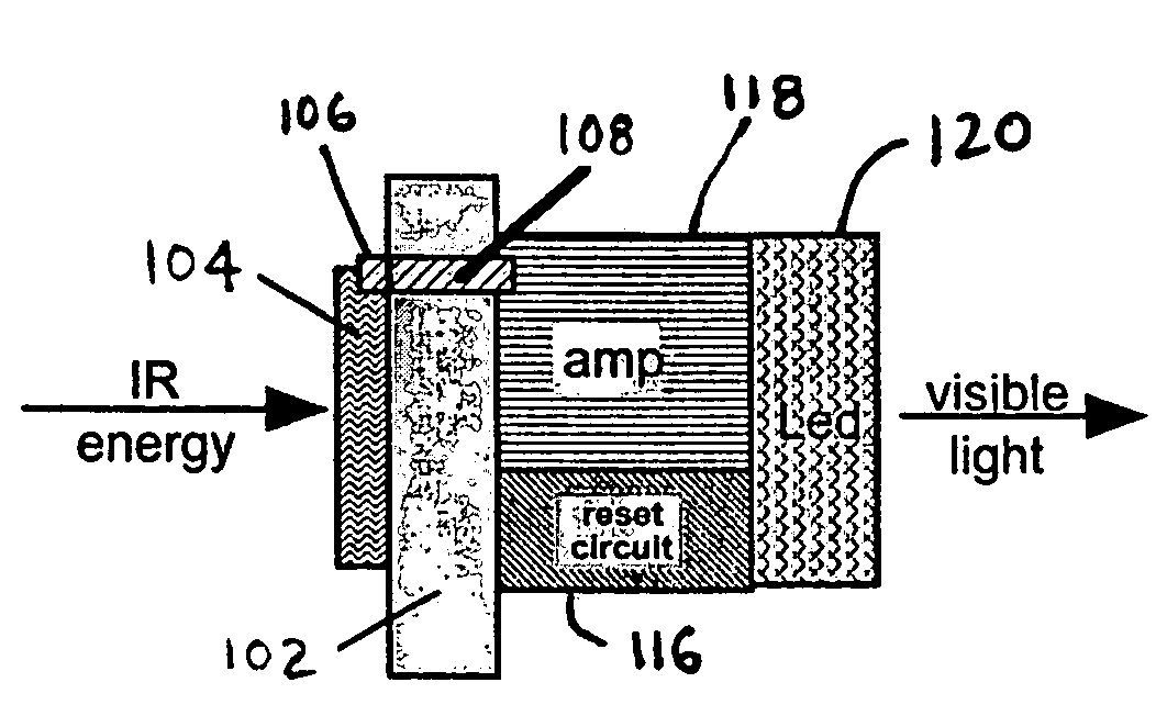
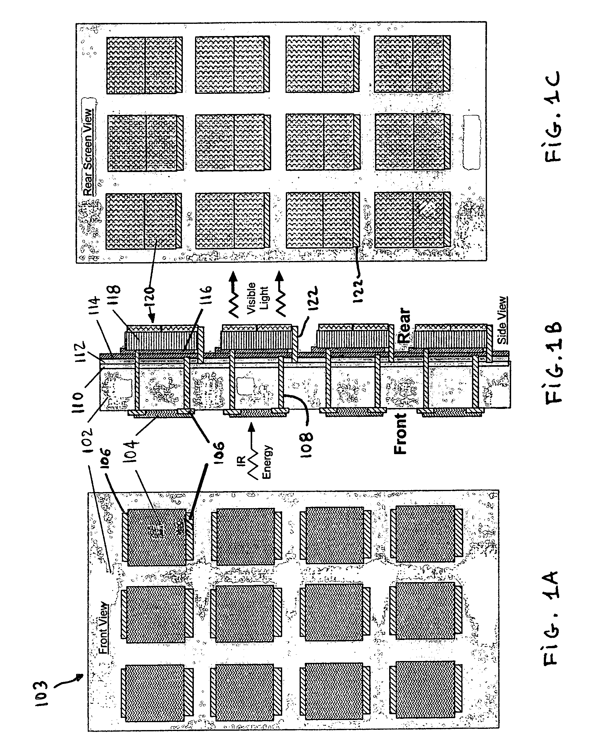
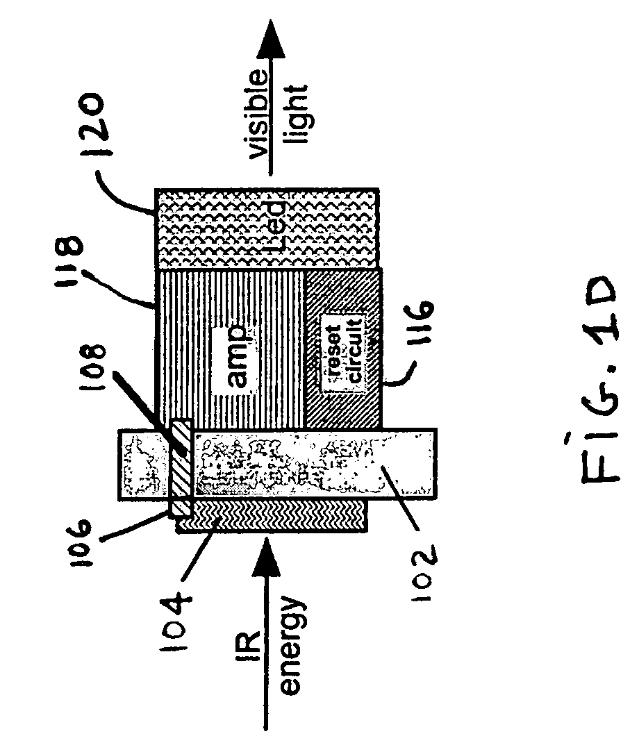
[0054]Embodiments of the present invention are described herein in the context of an infrared detector. Those of ordinary skill in the art will realize that the following detailed description of the present invention is illustrative only and is not intended to be in any way limiting. Other embodiments of the present invention will readily suggest themselves to such skilled persons having the benefit of this disclosure. Reference will now be made in detail to implementations of the present invention as illustrated in the accompanying drawings. The same reference indicators will be used throughout the drawings and the following detailed description to refer to the same or like parts.

[0055]In the interest of clarity, not all of the routine features of the implementations described herein are shown and described. It will, of course, be appreciated that in the development of any such actual implementation, numerous implementation-specific decisions must be made in order to achieve the de...


PUM


Abstract

A room temperature infrared imager, fabricated using MEMS (Micro Electro Mechanical Systems) techniques, made up of individually functioning analog elements laid out in a horizontal and vertical block matrix (pixel array). The front of each individual pixel element is IR sensitive and varies its properties in proportion to the corresponding analog level of incident IR energy exposure. An image infrared energy is focused across the front of the array to ultimately create a visible light image. The detector elements are formed on the front of a substrate. On the rear of the substrate, right behind the detectors, are electronics which read the sensors exposure level. Formed on top of the electronics are Light Emitting Devices (LED's). The electronics vary the brightness of the LED's proportionally with the exposure level on the front of the detector. The image is formed by the different visible light levels that appear on the array readout.

Description

CROSS-REFERENCE TO RELATED APPLICATIONS[0001]This application claims the benefit of U.S. Provisional Application No. 60 / 490,289, filed Jul. 25, 2003.FIELD OF THE INVENTION[0002]The present invention relates to imaging devices. More particularly, the present invention relates to infrared thermal imaging devices and thermal imaging sensors and detectors.BACKGROUND OF THE INVENTION[0003]Security and safety issues capture front-page coverage every day and have a growing impact on the US economy and quality of life. The average US citizen is seriously concerned about his family's risk of exposure to accidents, crime and acts against society.[0004]Infrared (IR) thermal imaging systems have been proliferating in commercial, but mostly industrial and military products. These devices have become less expensive over the last several years but are still too expensive to become mainstream products for widespread consumer use. The need for consumer-priced infrared thermal imaging equipment has n...

Claims


Application Information

Patent Timeline
Patent Type & Authority Patents(United States)
IPC IPC(8): H01L25/00
CPCH01L25/167G01J5/0215G01J5/0896G01J2005/0077H01L2924/3011H01L2924/0002H01L2924/00
Inventor KAUFMAN, PETER
Owner PUBLIC SERVICE SOLUTIONS
Why Eureka
Try Eureka