Low thermal resistance LED package

a low-temperature, led-based technology, applied in the direction of semiconductor devices, semiconductor/solid-state device details, electrical apparatus, etc., can solve the problems of excessive thermal resistance, limited thermal resistance, and high so as to reduce the thickness of the package, reduce the production cost of led-based packages, and reduce the thermal resistance of led-based packages

Active Publication Date: 2008-06-03
PROLIGHT OPTO TECH +1
View PDF1 Cites 53 Cited by
  • Summary
  • Abstract
  • Description
  • Claims
  • Application Information

AI Technical Summary

Benefits of technology

[0017]An object of this invention is to reduce the thermal resistance of a LED package. Another object of this invention is to reduce the production cost of LED package by reducing the thickness of the package.
[0019]The submount 20 is a section of the overall lead frame. The thickness is much smaller than prior art, the thermal resistance is much lower, and the process is simpler in that the extra step to insert a heat sink is eliminated. Although the instantaneous temperature rise is quicker, the final temperature is the same.
[0020]Another provision of the present invention is the installation of a highly transparent lens 22. The lens can be fabricated with resin, silicon, glass, Teflon, their composite or any other transparent material. The lens can reduce total internal reflection to increase luminance, and can change light pattern to satisfy different optical requirements.

Problems solved by technology

Due to the high price of gold, the cost is substantial in production.
The stress, which such wires can withstand, is limited, especially for the currently popular solderless bonding.
The stress produced by the solderless bonding causes higher temperature at the bond, which, in turn, may cause breakage.
These two structures all have the drawback that the thermal resistance is excessive.
When heating sinking is inadequate, the LED chip temperature rises, shortens the life of the LED, reduces the brightness of the light, and even causes the light source to be ineffective.
The printed circuit board shown in prior art FIG. 2 is made of plastic material, which has a very low thermal conductivity coefficient, and is incapable of dissipating heat.
When the energy is high, the LED can easily be overheated.
However, the conduction path is long and can only achieve a thermal resistance of 50-75° C. / W.
However, from a production stand point, the additional heat sink increases the production processing step and the height of the package.
Another problem is that when large LED chips are used, the packaging area need to be increased.
An increase in packaging area increases the stress caused by different expansion coefficients, and the danger of breaking the bonding wire also increases.

Method used


Image

  • Low thermal resistance LED package
  • Low thermal resistance LED package
  • Low thermal resistance LED package

Examples


second embodiment

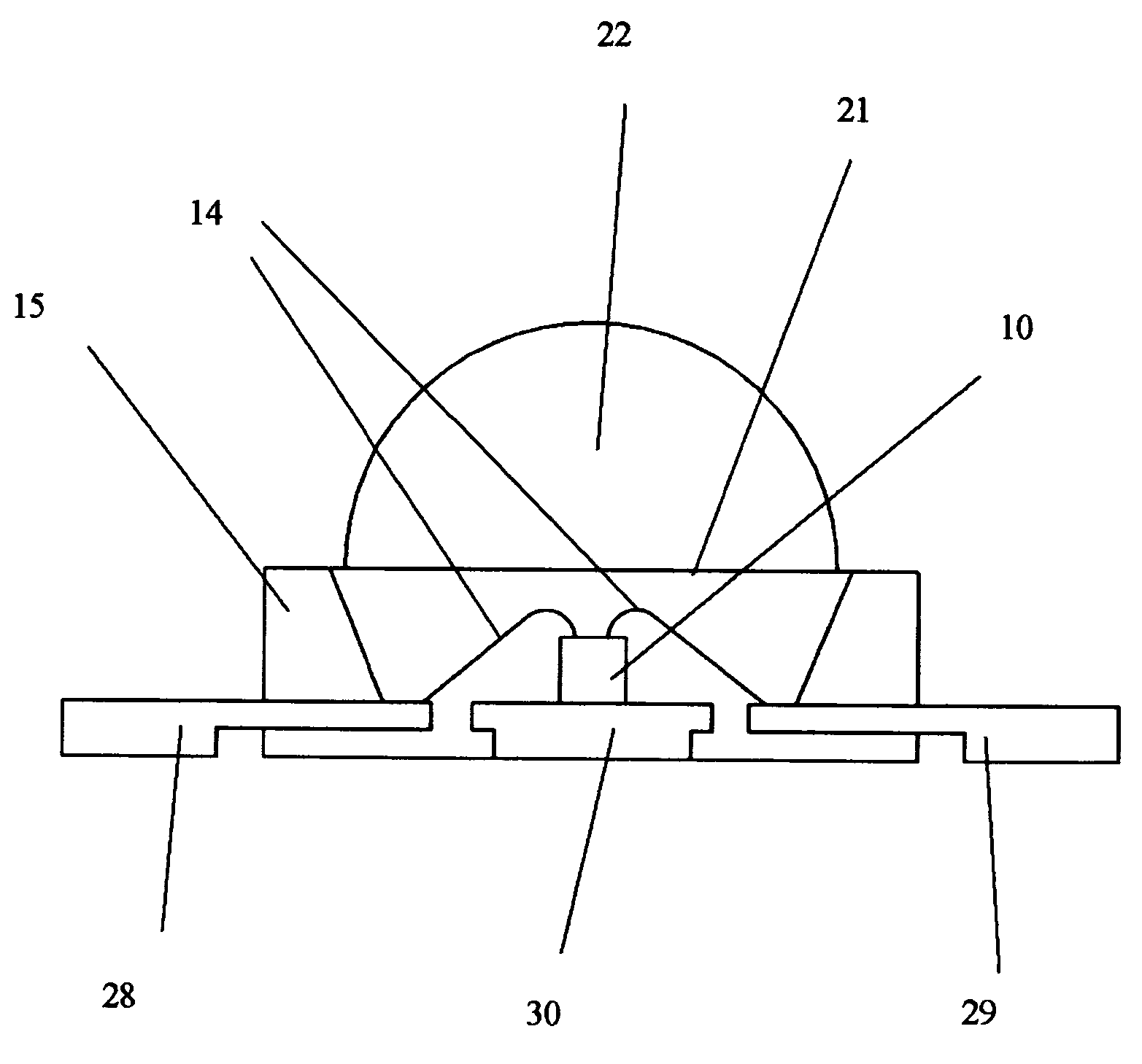
[0032]FIG. 6 shows the present invention. The structure is similar to that in FIG. 5, except that the three 0.5 mm metal sections are further half-etched from the bottom to from a positive lead frame 28, a negative lead frame 29 and a LED chip submount 30. The half-etched sections 28, 29 and 30 let the binding glue 15 to flow under half-etched sections to solidify the structure. Other elements with same reference numerals correspond to the same functions as that in FIG. 5.

third embodiment

[0033]FIG. 7 shows the present invention. A 0.5 mm thick metal sheet is punched out into five isolated sections: three positive lead frames 48, a negative lead frame 49, and a submount 40 for three color LEDs 10 which emit red, green and blue color lights. A glue is used to bind the five sections together and to form a cup with portions of the lead frames 48, lead 49 and the top of the submount 40 exposed, as shown in the cross-sectional view FIG. 8. The three LED chips 10 are mounted on the submount 40 and wire bonded with bonding wires 14 to respective positive lead frames 48 and common negative lead frame 49. Otherwise, the structure is similar to that in FIG. 6. Silicone 21 is used to fill the cup so as to cover and LED chips 10 and to protect the bonding wires 14. A convex lens is mounted over the silicone 21.

fourth embodiment

[0034]FIG. 9 shows the present invention. The structure is similar to that in FIG. 6 except that a back-to-back Zener diode 23 has been added for electric static protection. In this FIG. 8, the lead frame 58 corresponds to lead frame 28 in FIG. 6; lead frame 59 corresponds to lead frame 29; and lead frame 58 also corresponds to lead frame 30 in FIG. 6 in that this positive lead frame also serves as a connection to a terminal for the Zener diode 23. The other terminal of the Zener diode 23 is wire bonded to lead frame 59. Thus the Zener diode 23 is connected in parallel with the LED10. The elements with the same numerals correspond to the same functions as that in FIG. 6.


PUM


Abstract

A LED chip is bonded on a large submount serving as a heat sink. The submount is punched out from a thin metal sheet together with two other sections of lead frames for the LED and held together with insulating material. The planar structure makes the package thin. A transparent lens may be mounted over the submount. More than one LED of same or different color can be mounted on the submount.

Description

BACKGROUND OF THE INVENTION[0001]1. Field of the Invention[0002]This invention relates to light emitting diodes (LED), particularly to the packaging of LED for low thermal resistance.[0003]2. Brief Description of Related Art[0004]A traditional LED package is shown in FIG. 1. A LED chip 10 is mounted in a recess of a lead frame 11. The recess reflects the light emitted from the LED chip 10. The LED 10 is wire bonded with a gold wire or an aluminum wire 14 to another lead frame 11 to serve as a second terminal for the LED 10. The LED 10 is coated with transparent glue, leaving only the leads exposed for external connection. Such a LED package is widely used for traffic signal lights, signal lights in a car, and indicators in an electronic production line.[0005]Another prior art is shown in FIG. 2. A LED chip 10 is mounted on a printed circuit board 13, and is wire bonded with gold or aluminum wire 14 to surface contact leads of the printed circuit board. The structure is covered with ...

Claims


Application Information

Patent Timeline
Patent Type & Authority Patents(United States)
IPC IPC(8): H01L33/00H01L33/48H01L33/62H01L33/64
CPCH01L33/642H01L33/486H01L33/62H01L33/647H01L2224/48091H01L2224/48247H01L2924/01079H01L2924/00014H01L2224/45124H01L2224/45144H01L2224/45147H01L2924/01019H01L2924/12041H01L24/45H01L2924/01015H01L2924/00H01L2224/45015H01L2924/12035H01L2924/181H01L2224/49113H01L2224/48111H01L2924/00012
Inventor HSIN CHEN, CHEN-LUN
Owner PROLIGHT OPTO TECH
Why Eureka
Try Eureka