

Methods to self-synchronize clocks on multiple chips in a system
a clock and chip technology, applied in multiplex communication, instruments, generating/distributing signals, etc., can solve the problems of not being able to achieve the same system size and package/process limitation as the original approach, and not being able to meet the requirements of larger systems, so as to reduce the risk and requirement
Inactive Publication Date: 2008-06-03
INT BUSINESS MASCH CORP
View PDF3 Cites 18 Cited by
- Summary
- Abstract
- Description
- Claims
- Application Information
AI Technical Summary
Benefits of technology
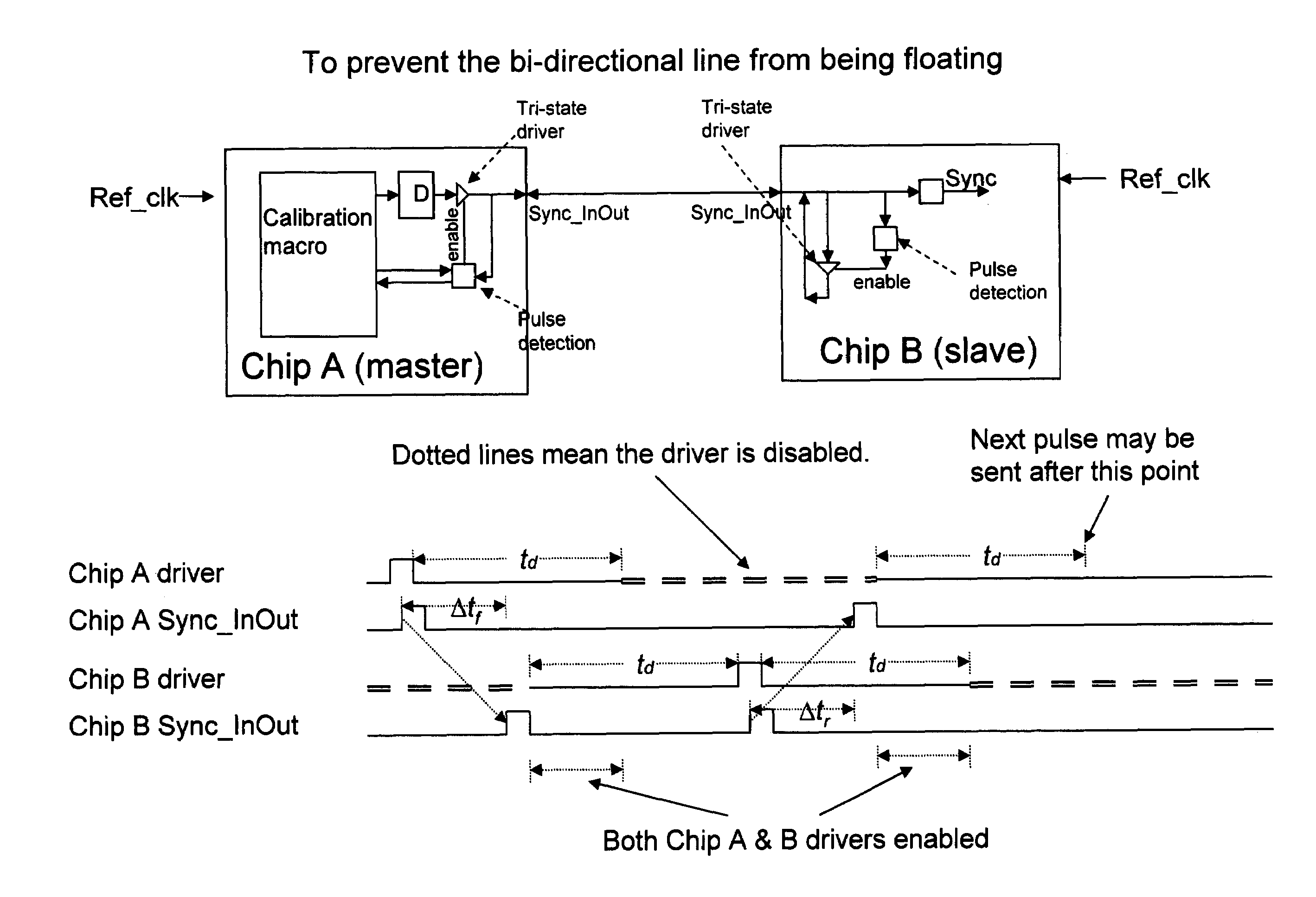
[0010]To remove the limitation on chip-to-chip communication latency matching and to account for various package variations, a simple set of training procedures may be applied prior to sending out synchronization signals to determine the actual latency from one master chip to a slave chip. The information is then applied to the timing of the synchronization signal for that particular slave chip. Since the latency between the master chip and each slave chip is individually measured, the timing of the synchronization signals to each slave chip may be individually adjusted. Any mismatch in the wiring path on the package for the synchronization signals will be accounted for in the proposed procedures. This is also true for package variations.
[0011]The main advantage of this invention is to enable the synchronization across chips in larger system that have synchronization signal latencies of different numbers of reference clock cycles. This situation can not be resolved in the approaches mention in the prior arts. Another advantage is to reduce the risk and requirement from packaging design, which is usually not as precise as the chip design. If lower quality packages are used, large variations of latency from one package to another may be accounted for with this invention. An additional advantage is that when a new packaging design is used with the same chips, no new packaging analysis is required. This is particularly helpful when the packaging design is done by less proficient customers.
Problems solved by technology
The simple synchronization approach described above no longer guarantee successful synchronization among all chips, since each chip may need different number of reference cycle to receive the synchronization signals.
But this approach still has the same limitation as the original approach in term of system size and package / process variations.
Additional work on package design may be required to match the latencies of synchronization signals among all chips, which may not feasible in larger systems.
Method used
View moreImage
Smart ImageViewing Examples

Examples
example
[0029]
Login to View More PUM
 Abstract
A method of self-synchronizing clocks in a multiple chip system, by assigning one chip as the master chip and the other chips as slave chips. A training signal is sent from master chip to the slave chips to determine the latency from the master chip to a slave chip, and then a synchronization signal is sent out to synchronize the “time zero” of the chips.
Description
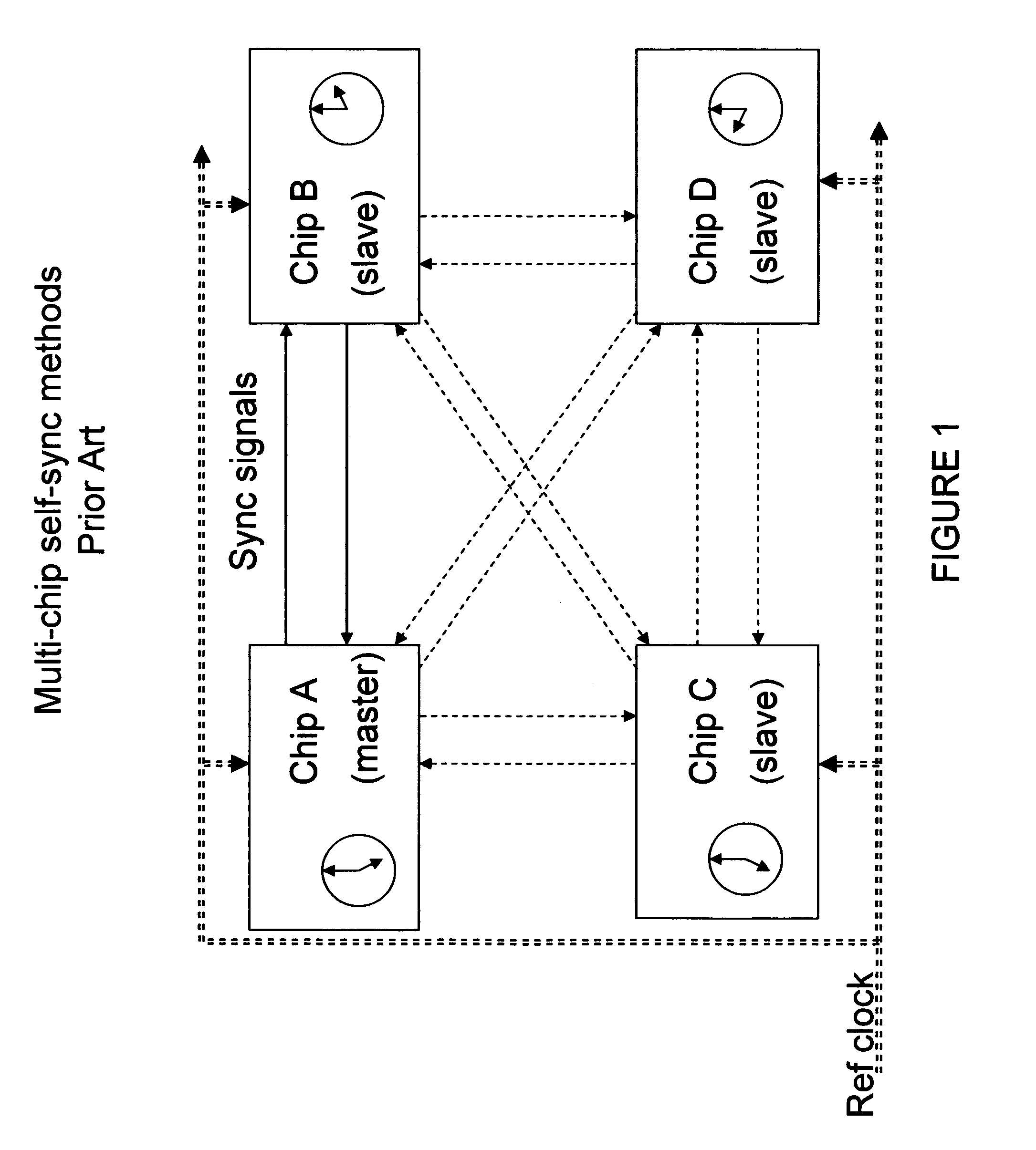
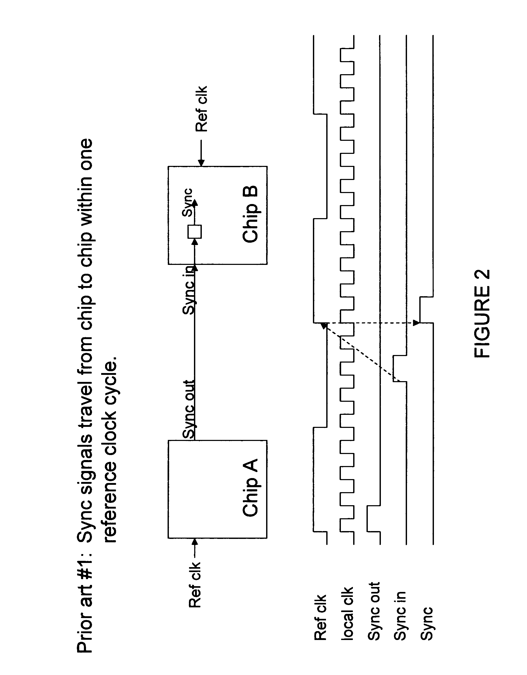
BACKGROUND[0001]1. Field of the Invention[0002]The invention relates to methods to self-synchronize clocks on multiple chips in a system[0003]2. Background Art[0004]A synchronous digital system consists of multiple chips that run on reference clocks with known relationship. Typically there are cross-chip functions that require the “time-zero” on each chip to be synchronized for the functions to work properly.[0005]In a multi-chip system, such as shown in FIG. 1, to synchronize all chips with each other without external controls, one chip may be temporarily assigned as the “master” chip. The rest of the chips will be “slave” chips. After a system is powered on, the master chip may start to send out synchronization signals to synchronize the “time-zero” of all slave chips and itself. The “time-zero” events usually are repeating with very long cycles. The timing of “time-zero” is typically aligned to the reference clock boundary assuming all chips are receiving the same reference clock...
Claims
Login to View More Application Information
Patent Timeline
 Patent Type & AuthorityPatents(United States)
IPC IPC(8): H04L7/00
CPCG06F1/10H03L7/06
InventorHWANG, CHARLIE C.MCNAMARA, TIMOTHY G.TONG, CHING-LUNGBECKER, WIREN DALE
OwnerINT BUSINESS MASCH CORP