Method for making a thermal interface material

a technology of thermal interface material and making method, which is applied in the direction of electrical apparatus construction details, indirect heat exchangers, lighting and heating apparatus, etc., can solve the problems of inadequately meeting the heat dissipation requirements of modern electronic components, the thickness of this kind of thermal interface material is limited to be greater than 40 micrometers, and the heat conduction coefficient of the thermal interface material is now considered too low for many contemporary applications

Active Publication Date: 2008-07-01
TSINGHUA UNIV +1
View PDF17 Cites 160 Cited by
  • Summary
  • Abstract
  • Description
  • Claims
  • Application Information

AI Technical Summary

Benefits of technology

[0010]However, the thermal interface material formed by injection molding is relatively thick. This increases a bulk of the thermal interface material and reduces its flexibility. Furthermore, the carbon nanotubes are disposed in the matrix material randomly and multidirectionally. This means that heat does not necessarily spread uniformly through the thermal interface material. In addition, the heat does not necessarily spread directly from the first surface engaged with the electronic element to the second surface engaged with the heat sink.

Problems solved by technology

However, a heat conduction coefficient of the thermal interface material is now considered to be too low for many contemporary applications, because it cannot adequately meet the heat dissipation requirements of modern electronic components.
However, the thickness of this kind thermal interface material is limited to be greater than 40 micrometers, and the heat conduction coefficient of the thermal interface material is inversely proportional to a thickness thereof.
The value of the heat conduction coefficient cannot be increased, because the thickness cannot be reduced.
However, the thermal interface material formed by injection molding is relatively thick.
This increases a bulk of the thermal interface material and reduces its flexibility.
This means that heat does not necessarily spread uniformly through the thermal interface material.

Method used


Image

  • Method for making a thermal interface material
  • Method for making a thermal interface material
  • Method for making a thermal interface material

Examples


Embodiment Construction

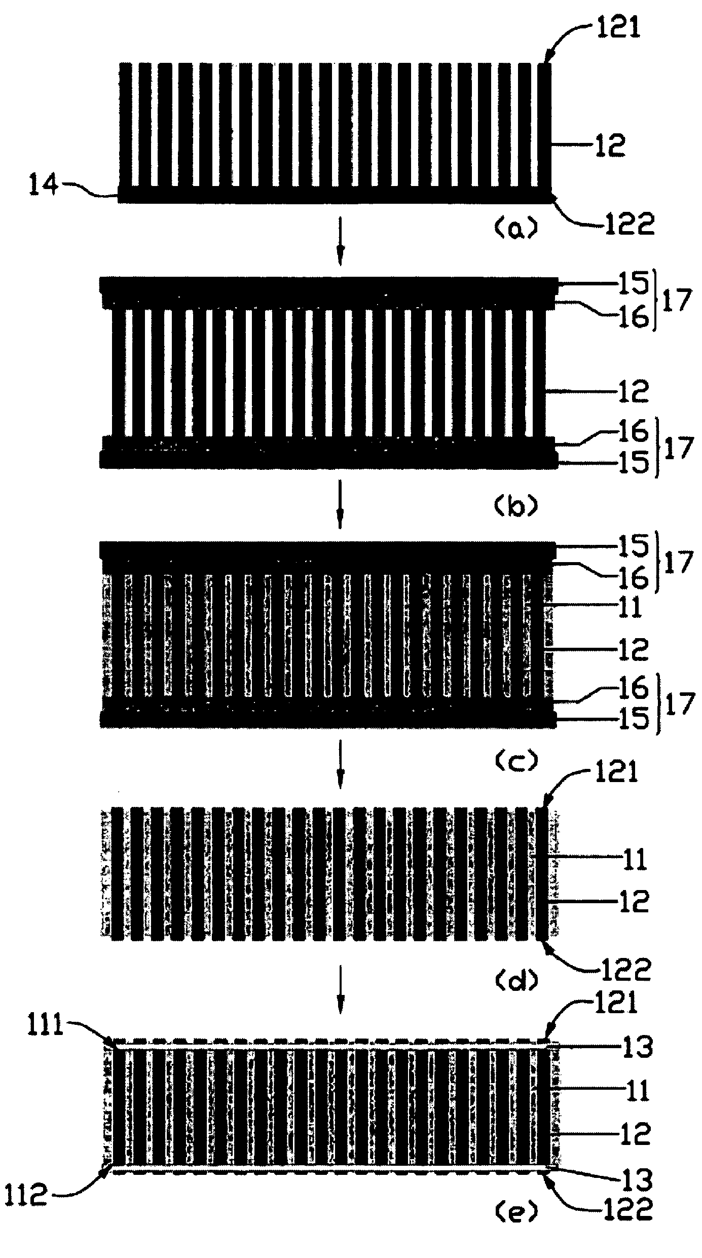
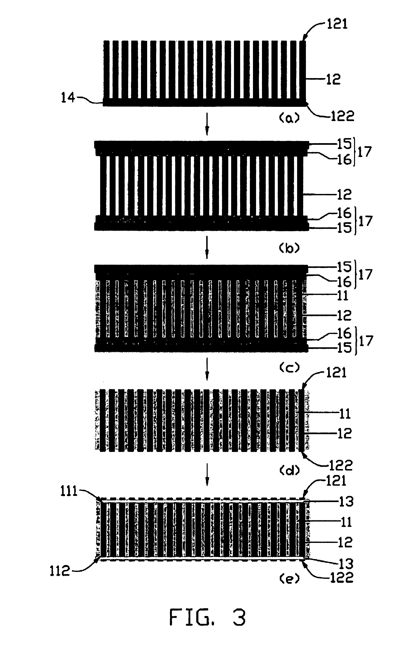
[0030]Embodiments of the present thermal interface material will now be described in detail below and with reference to the drawings.

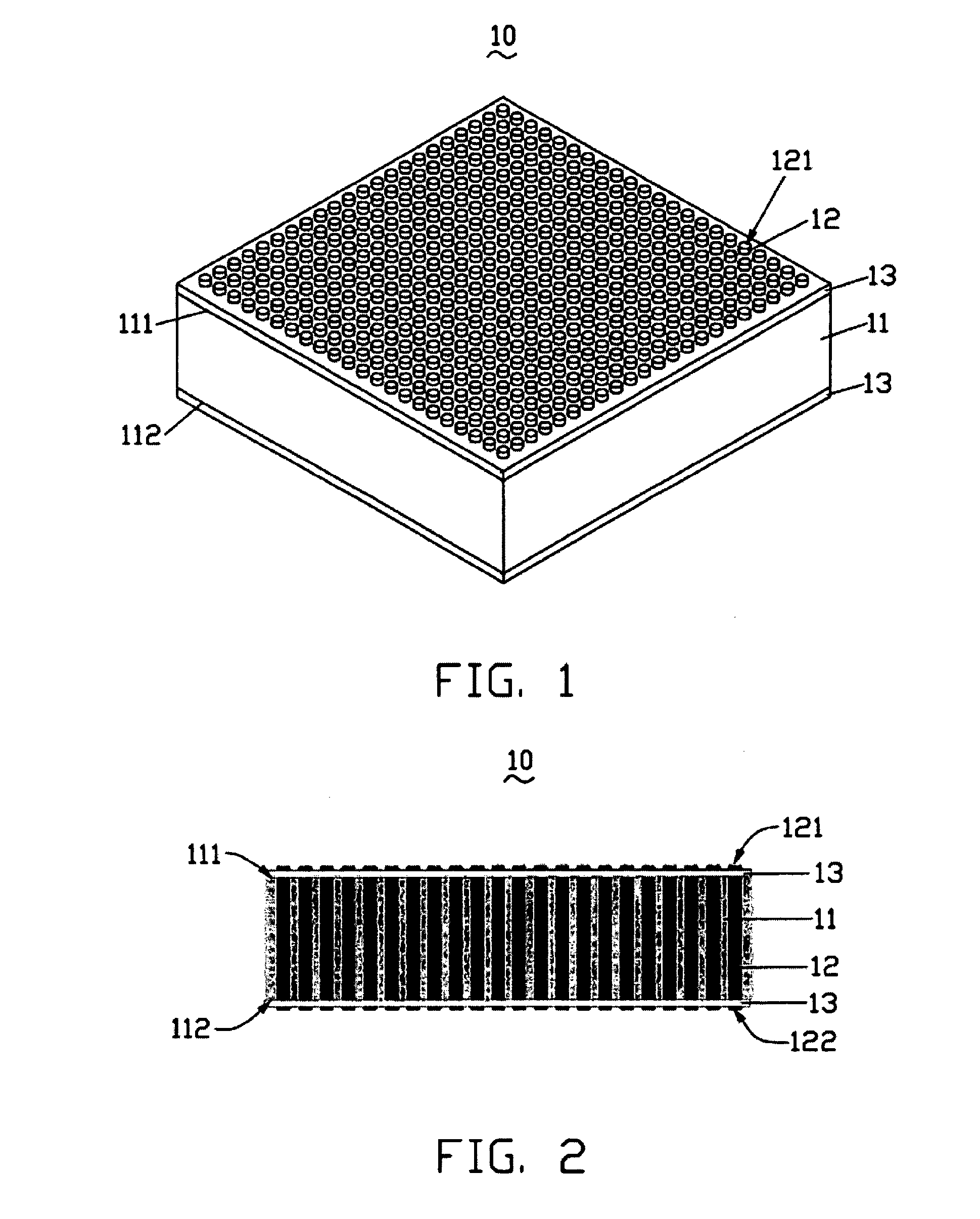
[0031]Referring to FIGS. 1 and 2, a thermal interface material (TIM) 10 includes a matrix 11, a plurality of carbon nanotubes (CNTs) 12, and dual phase change layers 13. The matrix 11 has a first surface 111 and an opposite second surface 112. The CNTs 12 are embedded in the matrix 11 uniformly. The CNTs 12 have a first end 121 and an opposite second end 122. The two opposite ends 121 and 122 are exposed out of the first and second surfaces 111, 112 of the matrix 11, respectively. The dual phase change layers 13 are formed on the two ends 121 and 122, respectively.

[0032]The first and second surfaces 111, 112 of the matrix 11 are substantially parallel to one another. The matrix 11 preferably has a thickness in the range from 1 to 1000 micrometers. In the preferred embodiment, the thickness of the matrix 11 is 20 micrometers. The matrix 11 is comprised,...


PUM

PropertyMeasurementUnit
thicknessaaaaaaaaaa
thicknessaaaaaaaaaa
thicknessaaaaaaaaaa

Abstract

A thermal interface material includes a matrix, a plurality of carbon nanotubes, and at least one phase change layer. The matrix includes a first surface and an opposite second surface. The carbon nanotubes are embedded in the matrix uniformly. The carbon nanotubes extend from the first surface to the second surface and have two opposite ends. At least one of the two opposite ends of the carbon nanotubes is exposed out of one of the first and second surfaces of the matrix. The at least one phase change layer is formed on the exposed end of the carbon nanotubes.

Description

CROSS-REFERENCES TO RELATED APPLICATIONS[0001]This application is related to four corresponding U.S. patent applications as follows: application Ser. No. 11 / 024,513, filed on Dec. 29, 2004, entitled “THERMAL INTERFACE MATERIAL AND METHOD FOR MANUFACTURING SAME”; application Ser. No. 11 / 025,160, filed on Apr. 21, 2005, entitled “METHOD FOR MANUFACTURING CARBON NANOTUBES WITH UNIFORM LENGTH”; application Ser. No. 11 / 089,864, filed on Mar. 25, 2005, entitled “THERMAL INTERFACE MATERIAL AND METHOD FOR MANUFACTURING SAME”; and application Ser. No. 11 / 321,278, filed on Dec. 29, 2005 entitled “THERMAL INTERFACE MATERIAL AND METHOD FOR MANUFACTURING SAME”; each of the above-identified applications having the same assignee as the instant application. The disclosures of the above-identified applications are incorporated herein by reference.BACKGROUND[0002]1. Technical Field[0003]The invention relates generally to thermal interface materials and making methods thereof; and more particularly to...

Claims


Application Information

Patent Timeline
Patent Type & Authority Patents(United States)
IPC IPC(8): B32B37/00
CPCF28D20/02F28F13/00F28F21/02H01L23/373H01L23/3737H01L2924/0002Y02E60/145F28F2013/006H01L2924/00Y02E60/14
Inventor HUANG, HUAWU, YANGLIU, CHANG-HONGFAN, SHOU-SHAN
Owner TSINGHUA UNIV
Why Eureka
Try Eureka