Method for fabricating self-aligned double layered silicon-metal nanocrystal memory element

a nanocrystal memory and silicon-metal technology, applied in the field of memory devices, can solve the problems of insurmountable difficulty in thinning-down process, difficult to store charges, and own limit of thinning-down process, and achieve the effect of enhancing the charge retention rate of nanocrystal memory, high work function, and increasing the potential barrier of nanocrystals

Inactive Publication Date: 2008-07-01
IND TECH RES INST
View PDF8 Cites 21 Cited by
  • Summary
  • Abstract
  • Description
  • Claims
  • Application Information

AI Technical Summary

Benefits of technology

[0013]Another objective of the present invention is to provide a method for fabricating an insulating layer to maintain the quantum confinement of the foregoing nanocrystal to enhance charge retention with combination of the advantage of higher data storing density of a metal nanocrystal.
[0019]As regards a self-aligned double layered silicon-metal nanocrystal memory element of the present invention, the silicon nanocrystals underlying the metal nanocrystals act as an insulating layer for quantum confinement, such that charges are confined to quantum wells and therefore unlikely to get lost. Moreover, the metal nanocrystals have relatively high work function, and thus potential barrier of the nanocrystals increases. The metal nanocrystals have more states in conduction band to store more charges. Thus potential energy does not increase and potential barrier does not decrease, after a charge has entered. Accordingly, charge retention of a nanocrystal memory is enhanced dramatically.

Problems solved by technology

However, whatever thinning-down effort is subject to the physical limit of direct tunneling, and thus a thinning down process does have its own limit.
The proposed nano-structure memory device overcomes a drawback of the prior art, that is, it is difficult to store charges (wherein charges are stored in polysilicon which forms a floating gate to achieve electric conduction in accordance with the prior art) in the presence of a current leakage from any point of a tunnel oxide layer underlying the conventional polysilicon floating gate.
Moreover, the conventional polysilicon floating gate achieves charge blocking solely by being barrier-dependent, thus causing insurmountable difficulty in a thinning-down process performed on the tunnel oxide layer.
Although the insurmountable difficulty in the foregoing design of the polysilicon floating gate is solved (by thinning down the tunnel oxide layer and thereby enabling charges to enter the quantum wells readily and thereby be stored), but charges stored in the silicon nanocrystal floating gate may readily tunnel out and hardly be retained, because disposed between the channel and the nanocrystals is a mere insulating layer, that is, the tunnel oxide layer.
With the double layered quantum well structure, after charges are stored in the nanocrystals, it is difficult for subsequent charges to enter the nanocrystals because of Coulomb blockade.
However, this method still has practical drawbacks.
Although its structural theory is better than the foregoing single layered nanocrystal, but insurmountable difficulty still exists in practice when fabrication parameter is considered.
If the previous level of the operating voltage is to be maintained or even lowered, the oxide layer will have to be thinned down, but the thinning down process will cause a memory retention problem.
Although memory retention can be enhanced if the thickness of the oxide layer is increased, the operating voltage is compromised.
For instance, it will be impossible to store enough charges in a nanocrystal layer disposed with nanocrystals, if the nanocrystals disposed in the nanocrystal layer are too small or over-dispersed; as a result, the charges present in a channel beneath an oxidation layer decrease, causing difficulty in interpretation.
In other words, in the event that few charges are stored in the nanocrystal layer, there will be a negligible difference between a threshold voltage associated with the presence of nanocrystals in the nanocrystal layer and a threshold voltage associate with the absence of nanocrystals from the nanocrystal layer, and in consequence it is impossible to determine whether charges are stored in the nanocrystal layer and perform effective interpretation.
According to current technology, it is difficult to increase nanocrystal density, and thus considerations are given to attempts to store more charges in each nanocrystal.
However, after a charge is stored in a nanocrystal, it is difficult for the next charge to enter the well and be stored in the nanocrystal because of an increase in potential energy.
Even if the charge is forcibly stored in the well, the barrier will be insufficient to stop the charge from tunneling out; as a result, the charge tunnels into an oxide layer and fails to be stored in the nanocrystal.

Method used


Image

  • Method for fabricating self-aligned double layered silicon-metal nanocrystal memory element
  • Method for fabricating self-aligned double layered silicon-metal nanocrystal memory element
  • Method for fabricating self-aligned double layered silicon-metal nanocrystal memory element

Examples


Embodiment Construction

[0036]The present invention, which relates to a self-aligned double layered silicon-metal nanocrystal memory element, a method for fabricating the same, and a memory having the memory element, is herein illustrated with the specific embodiments and drawings.

[0037]FIGS. 3A through 3G demonstrate a method for fabricating a self-aligned double layered silicon-metal nanocrystal memory element of the present invention.

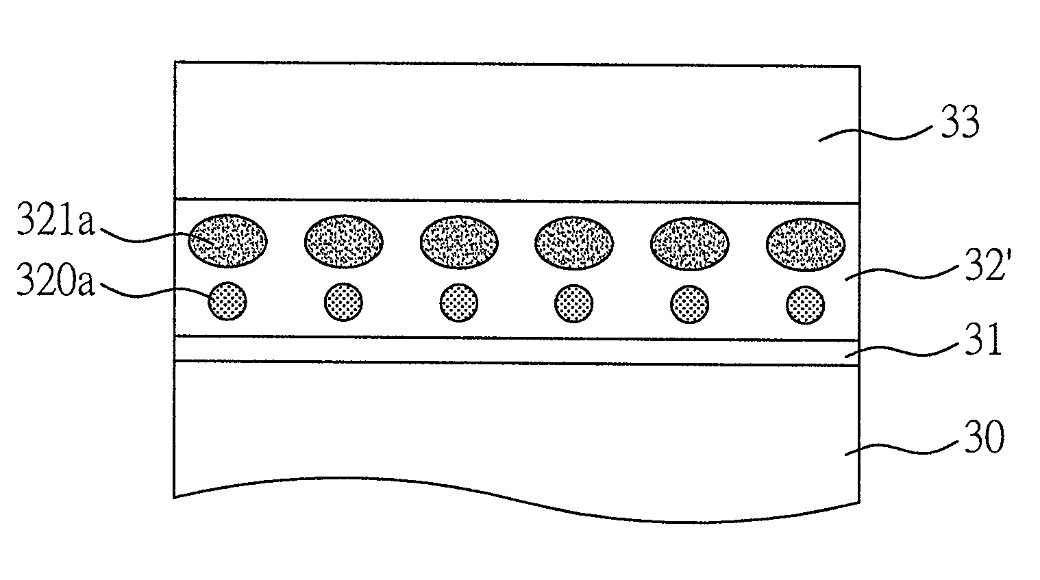
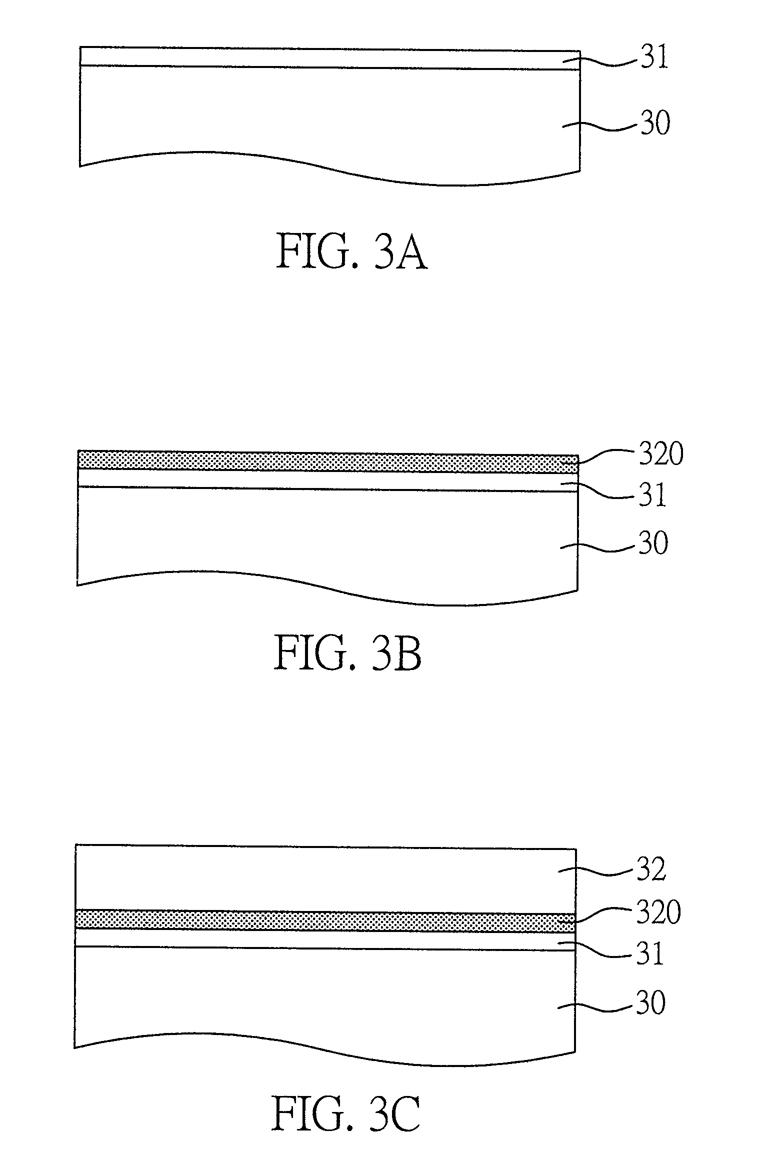
[0038]Referring to FIG. 3A, first of all, a tunnel oxide layer 31 is formed on a silicon-made substrate 30 by thermal oxidation known in the prior art. The tunnel oxide layer 31 may be made of silicon oxides or other dielectric materials and preferably 5 nanometers in thickness. The formation of the tunnel oxide layer 31 is an application of technology known in the prior art, and the constituent material is also known in the prior art, and thus it is not herein discussed in detail.

[0039]Moreover, referring to FIG. 3B, a polysilicon layer 320 is deposited on the tunnel oxide...


PUM


Abstract

A nanocrystal memory element and a method for fabricating the same are proposed. The fabricating method involves selectively oxidizing polysilicon not disposed beneath and not covered with a plurality of metal nanocrystals, and leaving intact the polysilicon disposed beneath and thereby covered with the plurality of metal nanocrystals, with a view to forming double layered silicon-metal nanocrystals by self-alignment.

Description

CROSS-REFERENCE TO RELATED APPLICATION[0001]This application claims the benefit of Taiwan Application No. 094138939, filed Nov. 7, 2005, the contents of which are hereby incorporated herein by reference in their entirety.FIELD OF THE INVENTION[0002]The present invention relates to a memory device and a method for fabricating the same, and more particularly, to a nanocrystal memory for accessing charges and a method for fabricating the same.BACKGROUND OF THE INVENTION[0003]Among existing non-volatile memory-based ICs, flash memory is the most advanced of its kind. A distinguishing feature of a conventional flash memory is that, in addition to an oxide insulating layer typically formed in a conventional MOSFET, a floating gate is formed in between a gate and a channel in the MOS of the tradition flash memory, such that data are stored by introducing into or removing from the floating gate negative charges. However, as regards conventional flash memory, the gate is made of doped polysi...

Claims


Application Information

Patent Timeline
Patent Type & Authority Patents(United States)
IPC IPC(8): H01L21/336
CPCB82Y10/00H01L21/28273H01L29/7881H01L29/66825H01L29/42332H01L29/40114
Inventor JENG, PEI-REN
Owner IND TECH RES INST
Why Eureka
Try Eureka