HIGH-k CAPPED BLOCKING DIELECTRIC BANDGAP ENGINEERED SONOS AND MONOS

a dielectric bandgap and high-k capped technology, applied in the field of flash memory technology, can solve the problems of limiting the ability to increase the density of flash memory, affecting the performance of flash memory, so as to improve the overall reliability, reduce the level of erase saturation, and improve the endurance and disturb characteristics of the device

Active Publication Date: 2009-03-05
MACRONIX INT CO LTD
View PDF84 Cites 23 Cited by
  • Summary
  • Abstract
  • Description
  • Claims
  • Application Information

AI Technical Summary

Benefits of technology

[0016]A blocking dielectric engineered, charge trapping memory cell is described having a dielectric stack between the gate and the channel including a charge trapping element that is separated from a gate by a blocking dielectric comprising a first layer in contact with the charge trapping element, such as silicon dioxide which can be made with high-quality, and a second layer in contact with said one of the gate and the channel, in which the second layer has a dielectric constant that is higher than that of the first layer, and preferably comprises a high-κ material, and more preferably a material having a dielectric constant more than 7. As described herein, the second layer has a dielectric constant κ2 higher than κ1 of the first layer, and the second layer has a thickness less than κ2 / κ1 times that of the first layer. This thickness relationship provides for use of a relatively thick first layer acting as a buffer layer, improving overall reliability, including charge retention, endurance and disturb characteristics of the device, while suppressing gate injection to reduce erase saturation levels.
[0017]As discussed in detail below, the electron barrier height and dielectric constant are both high in the interface with the gate, tending to suppress electron injection from the gate, while the layer contacting the charge trapping element acts as a buffer, masking defects in the other layer improving charge retention.

Problems solved by technology

As the density increases in memory devices, and the floating gate memory cells get closer and closer together, interference between the charge stored in adjacent floating gates becomes a problem.
This is limiting the ability to increase the density of flash memory based on floating gate memory cells.
However at that thickness, the endurance and charge retention characteristics of the memory cell are poor relative to traditional floating gate technology.
Also, with relatively thick tunneling dielectric layers, the electric field required for the erase operation also causes electron injection from the gate through the blocking dielectric layer.
However, if the erase saturation level is too high, the cell cannot be erased at all, or the threshold margin between the programmed and erased states becomes too small for many applications.
Decreasing the thickness of the tunneling dielectric layer is limited by issues of charge retention, as mentioned above.
However, the problem of the erase saturation continues to limit operational parameters of the device.
However, it is difficult to manufacture high-κ materials like aluminum oxide with high quality.
Of course, the use of silicon dioxide for the blocking layer results in the problem of high threshold erase saturation, because of the relatively high electric field magnitude in the lower κ material.
However, such high-κ materials tend to have defects, requiring that they be made relatively thick to prevent charge leakage or other reliability problems.
In general, the problem of electron injection from the gate during an erase bias intended to cause hole tunneling from the channel, which causes erase saturation, arises from the need to have a relatively high electric field in the tunneling layer.
Therefore, the benefits of these prior techniques are limited by the need to provide a thicker blocking dielectric layer.
However, a thin buffer oxide layer does not appear to provide substantial gains in retention and reliability without significant increases on the overall actual thickness of the blocking dielectric layer.
Furthermore, recent studies of the use of high-κ dielectrics show poor data retention for such cells, as shown for example by FIG. 7, of Chang et al., Reliability Characteristics of TANOS (TaN / AlO / SiN / Oxide / Si) NAND Flash Memory with Rounded Corner (RC) Structure”, Non-Volatile Semiconductor Memory Workshop, 2008 and 2008 International Conference on Memory Technology and Design.

Method used


Image

  • HIGH-k CAPPED BLOCKING DIELECTRIC BANDGAP ENGINEERED SONOS AND MONOS
  • HIGH-k CAPPED BLOCKING DIELECTRIC BANDGAP ENGINEERED SONOS AND MONOS
  • HIGH-k CAPPED BLOCKING DIELECTRIC BANDGAP ENGINEERED SONOS AND MONOS

Examples


Embodiment Construction

[0065]A detailed description of embodiments of the present invention is provided with reference to the FIGS. 1-34.

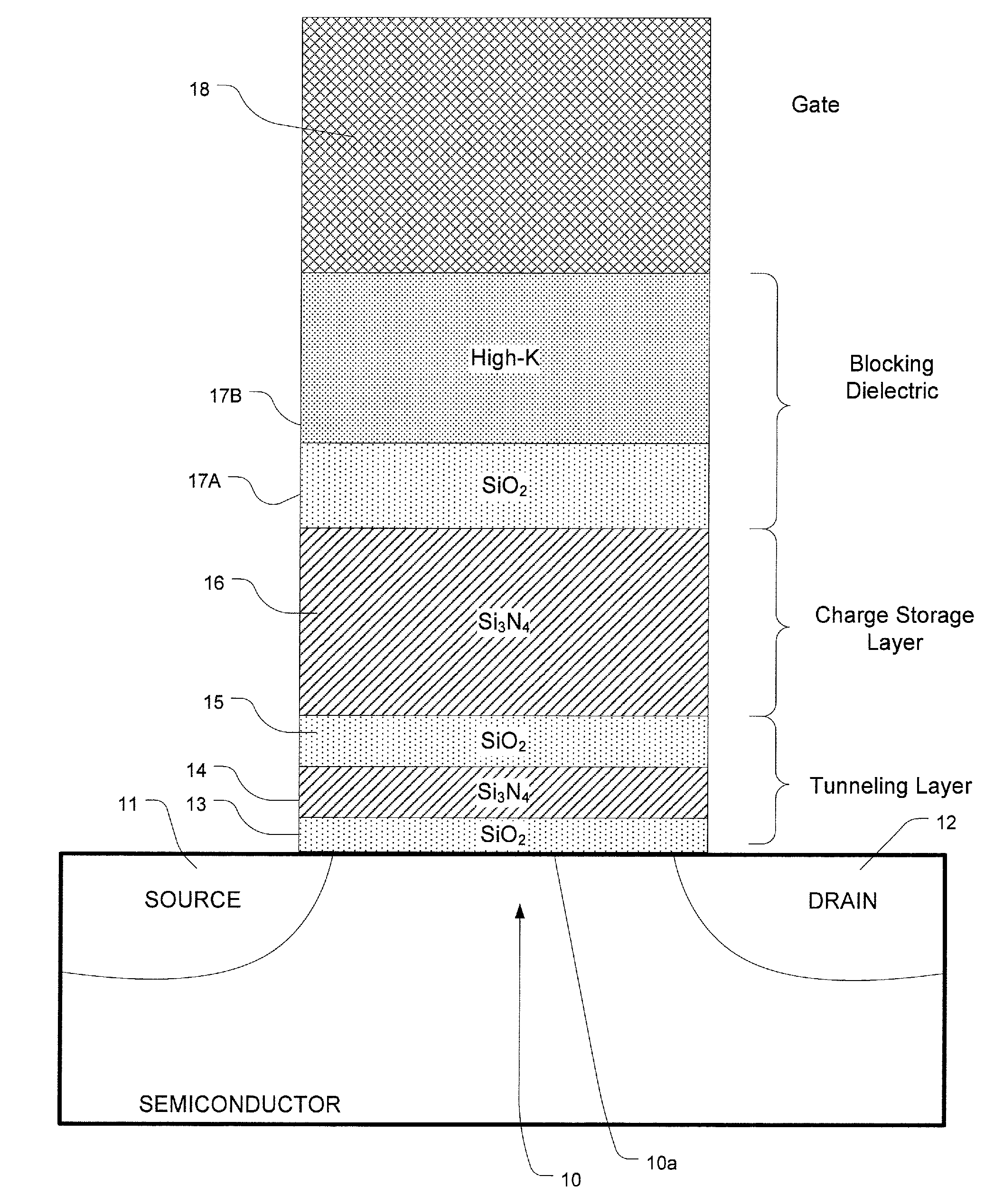
[0066]FIG. 1 is a simplified diagram of a charge trapping memory cell employing a multilayer blocking dielectric layer and a bandgap engineered dielectric tunneling layer. The memory cell includes a channel 10, a source 11 and a drain 12 adjacent the channel in a semiconductor body. A gate 18 overlies a multilayer stack, including the multilayer blocking dielectric layer, the charge trapping layer and the tunneling layer, of dielectric materials acting as the charge storage structure.

[0067]Gate 18 in this embodiment comprises p+ polysilicon. N+ polysilicon may also be used. Other embodiments employ metals, metal compounds or combinations of metals and metal compounds for the gate 18, such as platinum, tantalum nitride, metal silicides, aluminum or other metal or metal compound gate materials (e.g. from Ti, TiN, Ta, Ru, Ir, RuO2, IrO2, W, WN, and others. For some applicat...


PUM


Abstract

A blocking dielectric engineered, charge trapping memory cell includes a charge trapping element that is separated from a gate by a blocking dielectric comprising a buffer layer in contact with the charge trapping element, such as silicon dioxide which can be made with high-quality, and a second capping layer in contact with said one of the gate and the channel. The capping layer has a dielectric constant that is higher than that of the first layer, and preferably comprises a high-κ material. The second layer also has a conduction band offset that is relatively high. A bandgap engineered tunneling layer between the channel and the charge trapping element is provided which, in combination with the multilayer blocking dielectric described herein, provides for high-speed erase operations by hole tunneling. In an alternative, a single layer tunneling layer is used.

Description

CROSS REFERENCE TO RELATED APPLICATIONS[0001]The present application claims priority to U.S. Provisional Patent Application No. 60 / 968,076, filed on 27 Aug. 2007, and to U.S. Provisional Patent Application No. 61 / 019,178, filed on 4 Jan. 2008, each of which is incorporated by reference as if fully set forth herein.BACKGROUND OF THE INVENTION[0002]1. Field of the Invention[0003]The present invention relates to flash memory technology, and more particularly to scalable charge trapping memory technology adaptable for high speed erase and program operations.[0004]2. Description of Related Art[0005]Flash memory is a class of non-volatile integrated circuit memory technology. Traditional flash memory employs floating gate memory cells. As the density increases in memory devices, and the floating gate memory cells get closer and closer together, interference between the charge stored in adjacent floating gates becomes a problem. This is limiting the ability to increase the density of flash...

Claims


Application Information

Patent Timeline
Patent Type & Authority Applications(United States)
IPC IPC(8): G11C11/34H01L29/792H01L21/28
CPCG11C8/10G11C16/0466G11C16/0483H01L29/513H01L27/11568H01L29/4234H01L21/28282H01L29/40117H10B43/30H01L29/792
Inventor LAI, SHENG CHIHLUE, HANG-TINGLIAO, CHIEN WEI
Owner MACRONIX INT CO LTD
Why Eureka
Try Eureka