Methods of fabricating semiconductor device having capacitorless one-transistor memory cell

a semiconductor device and memory cell technology, applied in the direction of semiconductor devices, transistors, electrical appliances, etc., can solve the problem of limited data retention capability and operating characteristics of dram devices with such three-dimensional cell capacitors, and achieve the effect of improving data retention capability and operating characteristics

Active Publication Date: 2010-06-24
SAMSUNG ELECTRONICS CO LTD
View PDF58 Cites 131 Cited by
  • Summary
  • Abstract
  • Description
  • Claims
  • Application Information

AI Technical Summary

Benefits of technology

[0006]It is therefore a feature of an embodiment to provide a method of fabricating a semiconductor device having a capacitorless one-transistor memory cell exhibiting improved data retention capability and operating characteristics.

Problems solved by technology

High integration of such a three-dimensional cell capacitor may be limited in the DRAM device.

Method used


Image

  • Methods of fabricating semiconductor device having capacitorless one-transistor memory cell
  • Methods of fabricating semiconductor device having capacitorless one-transistor memory cell
  • Methods of fabricating semiconductor device having capacitorless one-transistor memory cell

Examples


Embodiment Construction

[0020]Korean Patent Application No. 10-2008-0129318, filed on Dec. 18, 2008, in the Korean Intellectual Property Office, and entitled: “Methods of Fabricating Semiconductor Device Having Capacitorless One-Transistor Memory Cell,” is incorporated by reference herein in its entirety.

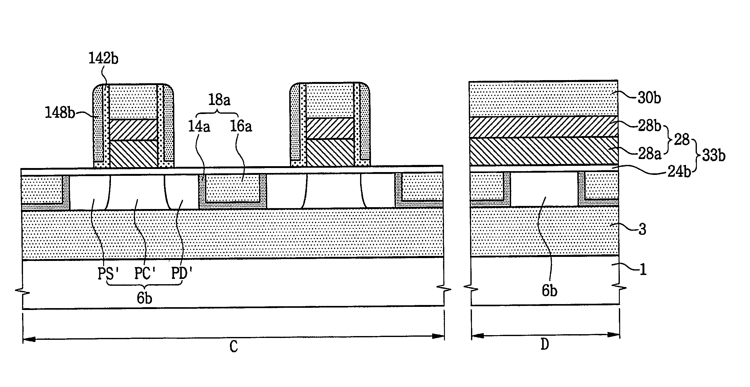
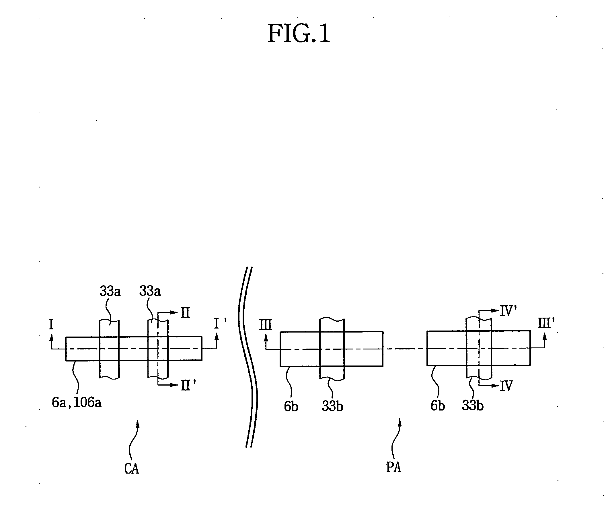
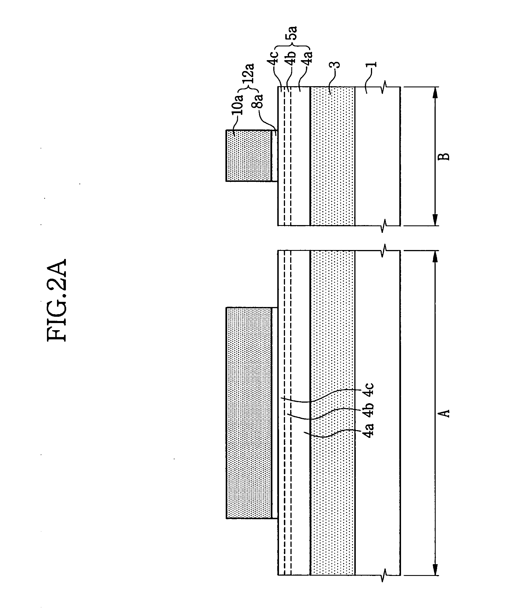
[0021]Example embodiments will now be described more fully hereinafter with reference to the accompanying drawings; however, they may be embodied in different forms and should not be construed as limited to the embodiments set forth herein. Rather, these embodiments are provided so that this disclosure is thorough and complete and fully conveys the scope of the inventive concept to one skilled in the art. In the drawings, the dimensions of layers and regions may be exaggerated for clarity of illustration. It will also be understood that when a layer is referred to as being “on” or “under” another layer or substrate, it can be directly on or under the other layer or substrate, or intervening layers may also...


PUM


Abstract

A method of fabricating a semiconductor device having a capacitorless one-transistor memory cell includes forming a first floating body pattern on a lower insulating layer of a substrate and a first gate pattern crossing over the first floating body pattern and covering sidewalls of the first floating body pattern is formed. The first floating body pattern at both sides of the first gate pattern is partially etched to form a protrusion portion extending between and above the partially etched regions, and first impurity regions are formed in the partially etched regions of the first floating body pattern.

Description

BACKGROUND[0001]1. Field[0002]Example embodiments relate to a method of fabricating a semiconductor device. More particularly, example embodiments relate to a method of fabricating a semiconductor device having a capacitorless one-transistor memory cell with improved data retention capability and operating characteristics.[0003]2. Description of Related Art[0004]A unit cell of a DRAM device may include a cell capacitor and an access transistor. In general, the cell capacitor is three-dimensionally formed by a complicated process. High integration of such a three-dimensional cell capacitor may be limited in the DRAM device. Therefore, research into data storage capable of replacing the three-dimensional cell capacitor has been underway.SUMMARY[0005]Embodiments are therefore directed to a method of fabricating a semiconductor device having a capacitorless one-transistor memory cell, which substantially overcomes one or more of the problems due to the limitations and disadvantages of t...

Claims


Application Information

Patent Timeline
Patent Type & Authority Applications(United States)
IPC IPC(8): H01L21/782
CPCH01L27/108H01L29/7841H01L27/10894H01L27/10802H10B12/20H10B12/00H10B12/09H10B99/00
Inventor SONG, HO-JUKIM, SUNG-HWANOH, YONG-CHUL
Owner SAMSUNG ELECTRONICS CO LTD
Why Eureka
Try Eureka