Method for testing power MOSFET devices

a technology of power mosfet and mosfet splice, which is applied in the direction of measuring devices, electrical testing, instruments, etc., can solve the problems of affecting the suitability of power mosfet, affecting the accuracy of power mosfet comparison, so as to achieve high reliability and uniformity, accurate predictor of power mosfet suitability, and high probability of passing

Inactive Publication Date: 2008-07-08
DOLIAN GRAPHICS
View PDF4 Cites 6 Cited by
  • Summary
  • Abstract
  • Description
  • Claims
  • Application Information

AI Technical Summary

Benefits of technology

[0018]The present invention uses characteristics of the gate charge waveform to test power MOSFETs in a new and unexpected way to produce a highly reliable and uniform testing methodology that replaces the inconsistent and inefficient dv / dt immunity testing currently performed. The test centers on the ratio of QGD over QGS1, where this ratio can be used for binning and sorting the devices. The ratio of QGD over QGS1 is a unique parameter to semiconductor testing as a substitute for more complicated and less reliable dv / dt immunity testing, and a very accurate predictor of a power MOSFET's suitability for a specified purpose. In particular, a semiconductor with a properly classified ratio of QGD over QGS1 has a very high probability of passing a comparible dv / dt immunity test for the intended application. The test will allow semiconductor manufacturers to assure its customers that properly selected and tested components will pass dv / dt immunity with greater yields and fewer failures. Because the gate charge parameters are relatively easily measured with high accuracy, and independent of test set-up or tester, reliability is far greater than previous methods and improved efficient results.
[0019]Using a second ratio of the gate charge waveform can further enhance the reliability and predictability of the testing procedure. For example, if QG is defined as the charge from t0 to the point on the gate charge waveform where the supply (or driving) voltage VGS is equal to the actual gate voltage of the device, the ratio of QGD over QG is a secondary predictor that when coupled with the first ratio further improves the accuracy of the method of the present invention. Other ratios employing QGmin, QGS1, QG, QGD, and QGS leads to even greater reliability and precision.

Problems solved by technology

Although input capacitance values are useful, they do not provide accurate results when comparing the switching performances of two devices from different manufacturers.
Rather, size effects and transconductance hinder such comparisons.
If this rate is exceeded, then the voltage across the gate-source terminals may become higher than the threshold voltage of the device, forcing the device into current conduction mode, and under certain conditions a catastrophic failure may occur.
From the foregoing, it is clear that devices with a low threshold voltage VTH are more prone to unwanted dv / dt turn-on.
While the data sheets of power MOSFETs include different specifications, most often some very important parameters such as gate resistance RG and gate charge QG are not directly measured despite directly affecting the switching performance of the devices.
The desired high switching frequencies are limited by the switching losses in the high-side MOSFET.
However, increasing the on and off transitions result in a more susceptible low-side MOSFET to dv / dt induced turn-on.
As stated above, when the applied dv / dt results in a gate voltage that exceeds the MOSFET gate-to-source threshhold voltage, the converter's reliability and overall efficiency suffers.
Although much work has gone into improving the dv / dt immunity test, it is still very unreliable and requires high limits or tolerance to be placed on the bands of acceptable components.
These high bands or tolerance lead to many viable and operable components being discarded for failing the tolerances limits, and the imprecision of existing testing still allows too high of a percentage of bad components to incorrectly pass the test and be delivered to customers.
A bad component is then typically installed into a larger component whose failure is much more costly than replacing the original semiconductor.
Further, a difficulty with present dv / dt testing is that it is highly test set-up sensitive, in that results vary widely from one set-up and one tester to another.
This disparity leads to inconsistency and higher limits to avoid the false positive passing of a bad component.

Method used


Image

  • Method for testing power MOSFET devices
  • Method for testing power MOSFET devices
  • Method for testing power MOSFET devices

Examples


Embodiment Construction

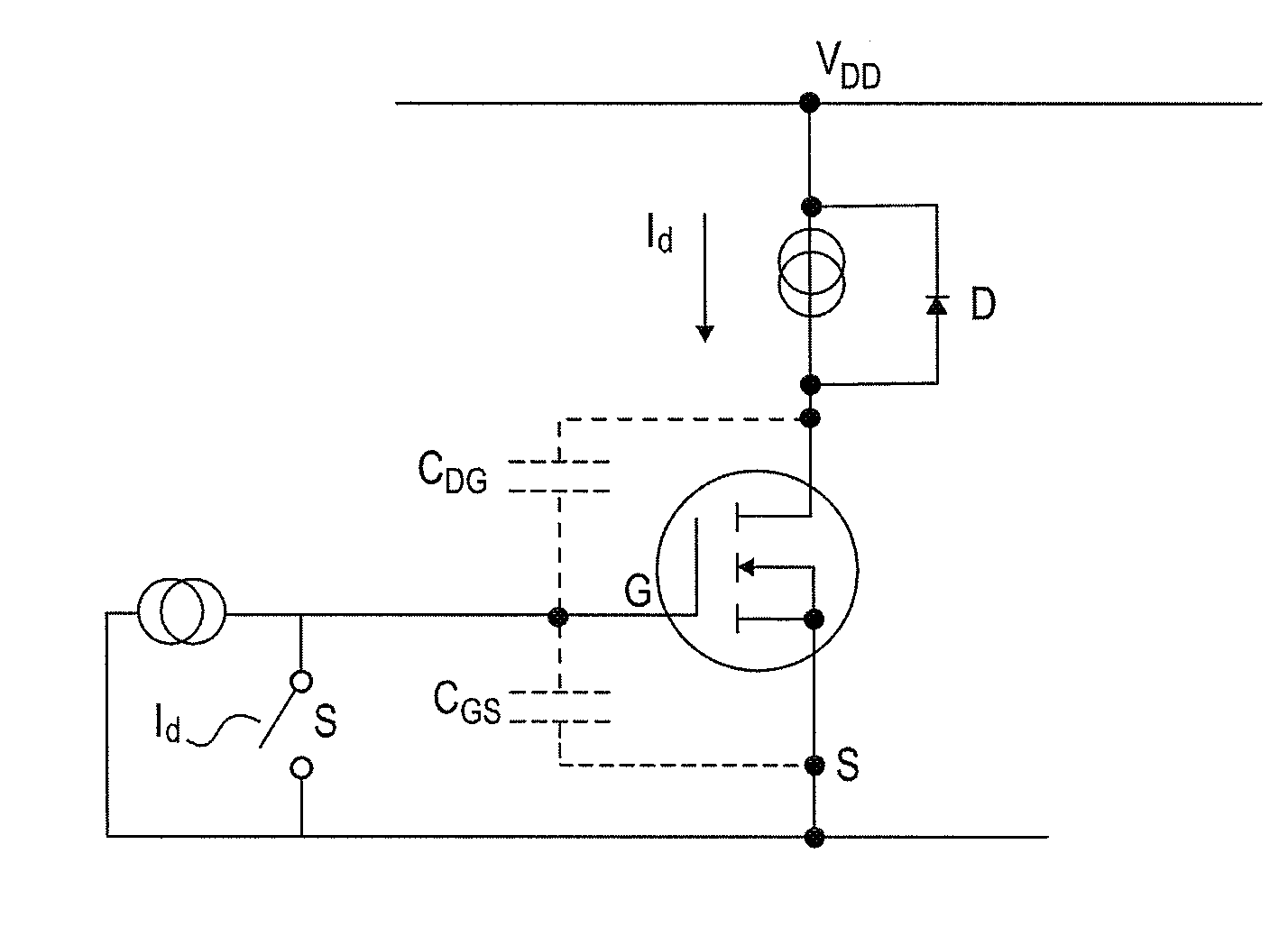
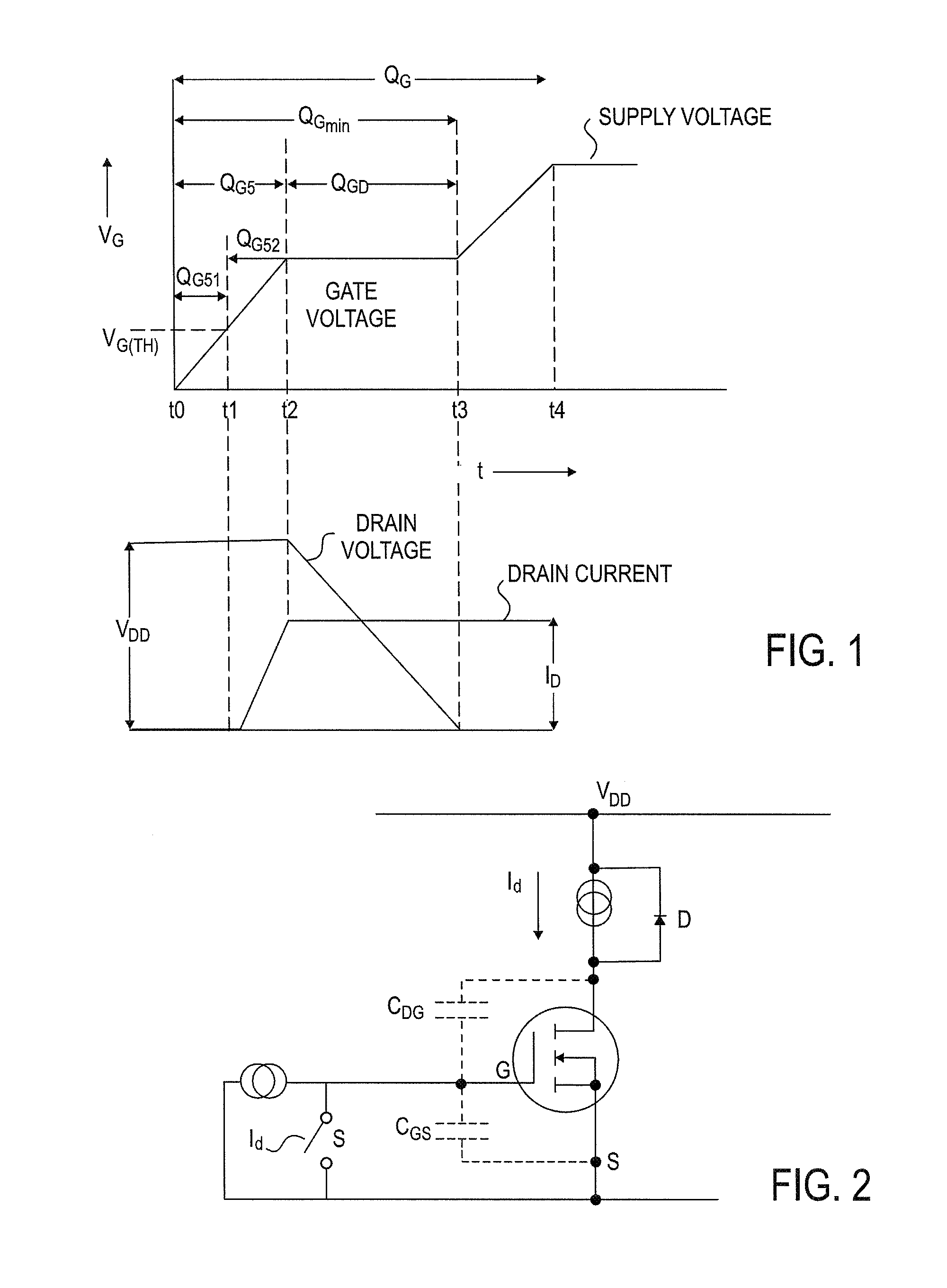
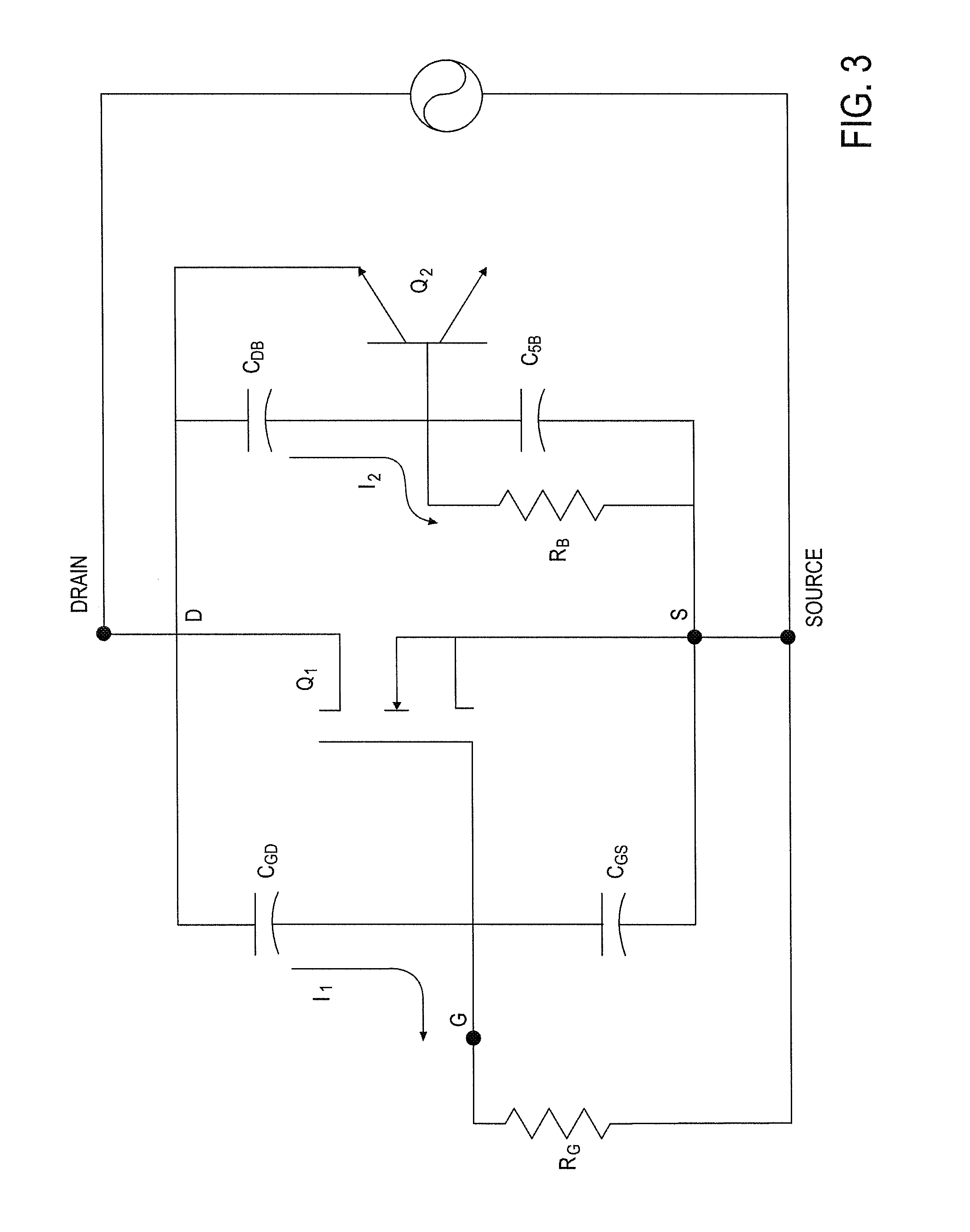
[0024]The structure of the power MOSFET is such that a parasitic bipolar transistor is inherent. Accordingly, N-channel MOSFET's include a parasitic NPN transistor, while P-channel MOSFET's include a parasitic PNP transistor. Under conditions where the rate of change of the Drain to Source voltage is below a given threshold, the parasitic transistor remains in the off state. However, in cases where the Drain to Source voltage changes rapidly, the parasitic transistor Q2 (see FIG. 3) may turn-on and provide a current conduction. When this occurs, current flow is limited to a small fraction of the semiconductor die. This in turn results in localized heating, which in many cases causes the destruction of the die and failure of the transistor.

[0025]Referring to FIG. 3, it is apparent that as the ratio of CDB / CSB is increased, the voltage applied to the base of transistor Q2 will be increased for a given rate of Drain voltage rise. Thus if CDB / CSB is less than a critical value, Q2 will n...


PUM


Abstract

Characteristics of a power MOSFET gate charge test waveform are evaluated to yield a highly reliable and uniform testing methodology that replaces the inconsistent and inefficient dv / dt immunity testing currently performed. The invention utilizes the ratio of QGD over QGS1 to replace traditional dv / dt immunity testing in order to perform binning and sorting the devices. The ratio of QGD over QGS1 has proven to be a very reliable substitute for standard dv / dt immunity tests, and a very accurate predictor of a power MOSFET's suitability for a specified purpose. Because the gate charge parameters are relatively easily measured with high accuracy, and independent of test set-up or tester, reliability is far greater than previous methods and improved efficient results. Additional ratios of charge parameters enhance the performance of the testing methodology of the present invention.

Description

FIELD OF THE INVENTION[0001]The present invention relates generally to the testing of semiconductor devices, and more particularly to a method for screening and binning power MOSFET devices based on specific ratios obtained from a gate charge waveform graph.BACKGROUND OF THE INVENTION[0002]The power semiconductor industry uses various tests to validate and categorize the product worthiness of a particular semiconductor for specific applications. The subject of the present invention is a novel testing system comprising a method and apparatus tailored to test power MOSFET devices in lieu of less reliable tests such as dv / dt immunity tests, leading to improved yields and more reliable validation.[0003]Metal oxide semiconductor field effect transistors (MOSFETs) are used in certain circuit applications as a control switch, where its purpose is primarily to control the drain current via the gate voltage. An overview of the structure of the MOSFET is well known in the art, and many refere...

Claims


Application Information

Patent Timeline
Patent Type & Authority Patents(United States)
IPC IPC(8): G01R31/26
CPCG01R31/2621
Inventor DOLIAN, KRIKOR M.
Owner DOLIAN GRAPHICS
Why Eureka
Try Eureka