Supercharge Your Innovation With Domain-Expert AI Agents!

Method of searching paths suffering from the electrostatic discharge in the process of an integrated circuit design

a technology of integrated circuit design and path searching, which is applied in the direction of program control, total factory control, instruments, etc., can solve the problems of high probability of damage to electronic devices, high probability of esd in soc, and damage to internal components of soc, so as to save time and cost of ic design

Inactive Publication Date: 2008-07-08
CHANG GUNG UNIVERSITY
View PDF4 Cites 2 Cited by
  • Summary
  • Abstract
  • Description
  • Claims
  • Application Information

AI Technical Summary

Benefits of technology

[0018]It is therefore one object of the invention to provide a method of searching paths that are susceptible to ESD at the beginning of an IC design. By utilizing this method, it is possible of greatly saving time and cost of the IC design.

Problems solved by technology

In manufacturing, assembling, packaging, and delivering of electronic devices and even at the time of using an electronic device by a user, there is pretty high probability of damaging the electronic device due to electrostatic discharge (ESD).
For example, when a deep submicron system-on-a-chip (SoC) is employed in a semiconductor manufacturing process, the SoC is susceptible to ESD.
Thus, internal components of SoC may be severely damaged by momentary unwanted currents.
However, even if the five principles are fully carried out, they cannot completely prevent the components of SoC from being damaged by ESD.

Method used


Image

  • Method of searching paths suffering from the electrostatic discharge in the process of an integrated circuit design
  • Method of searching paths suffering from the electrostatic discharge in the process of an integrated circuit design
  • Method of searching paths suffering from the electrostatic discharge in the process of an integrated circuit design

Examples


Embodiment Construction

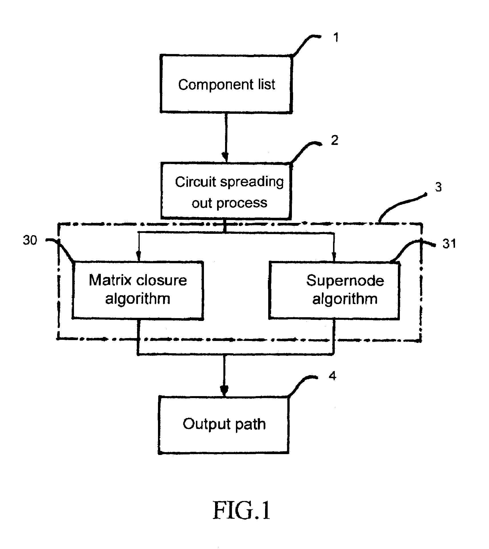
[0026]Referring to FIG. 1, a method of searching paths that are susceptible to electrostatic discharge (ESD) at the beginning of an integrated circuit (IC) design in accordance with the invention is illustrated.

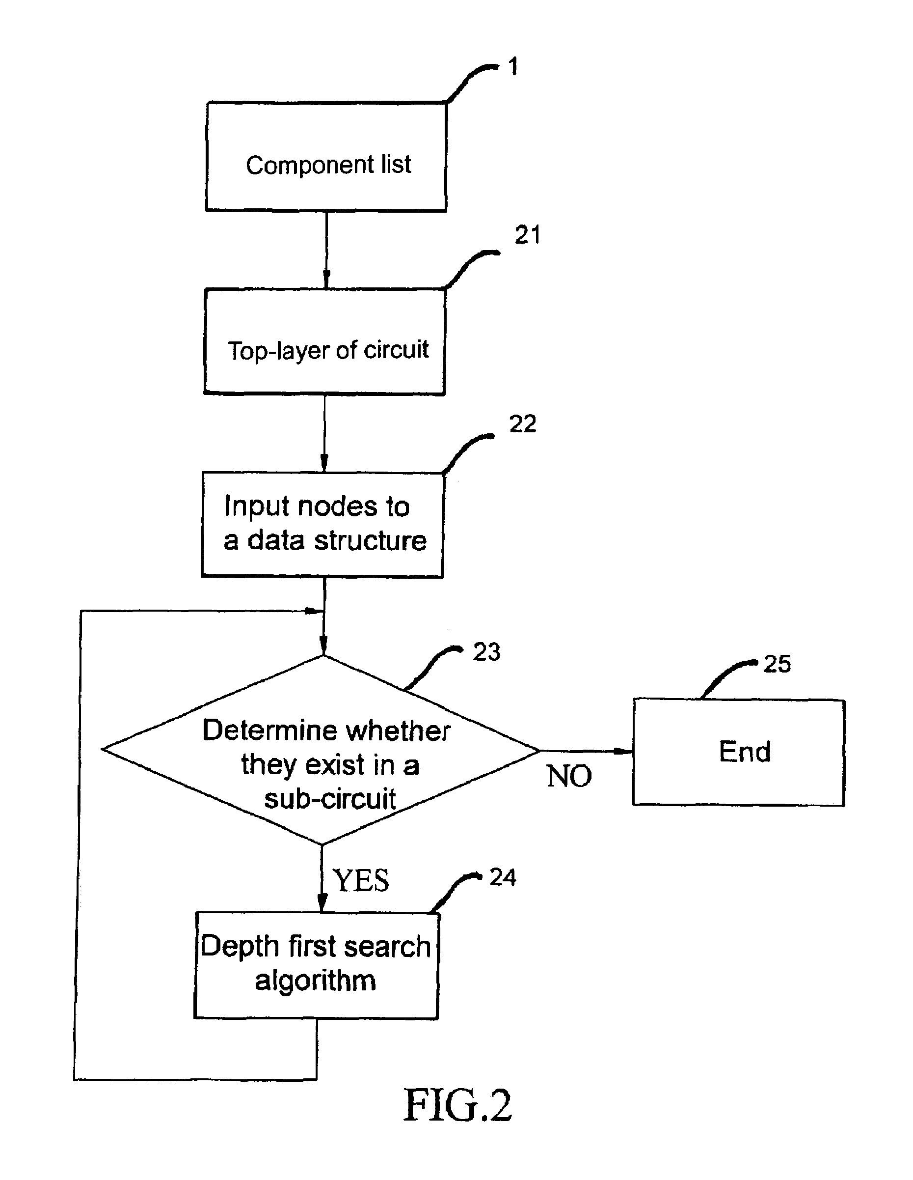
[0027]Component list in step 1 means data about resistors, inductors, capacitors, conductors, diodes, passive elements, and active elements such as metal-oxide semiconductors (MOSs) and the component list is fed to a computer for storage.

[0028]Circuit spreading out process in step 2 means spreading out circuit associated with the component list.

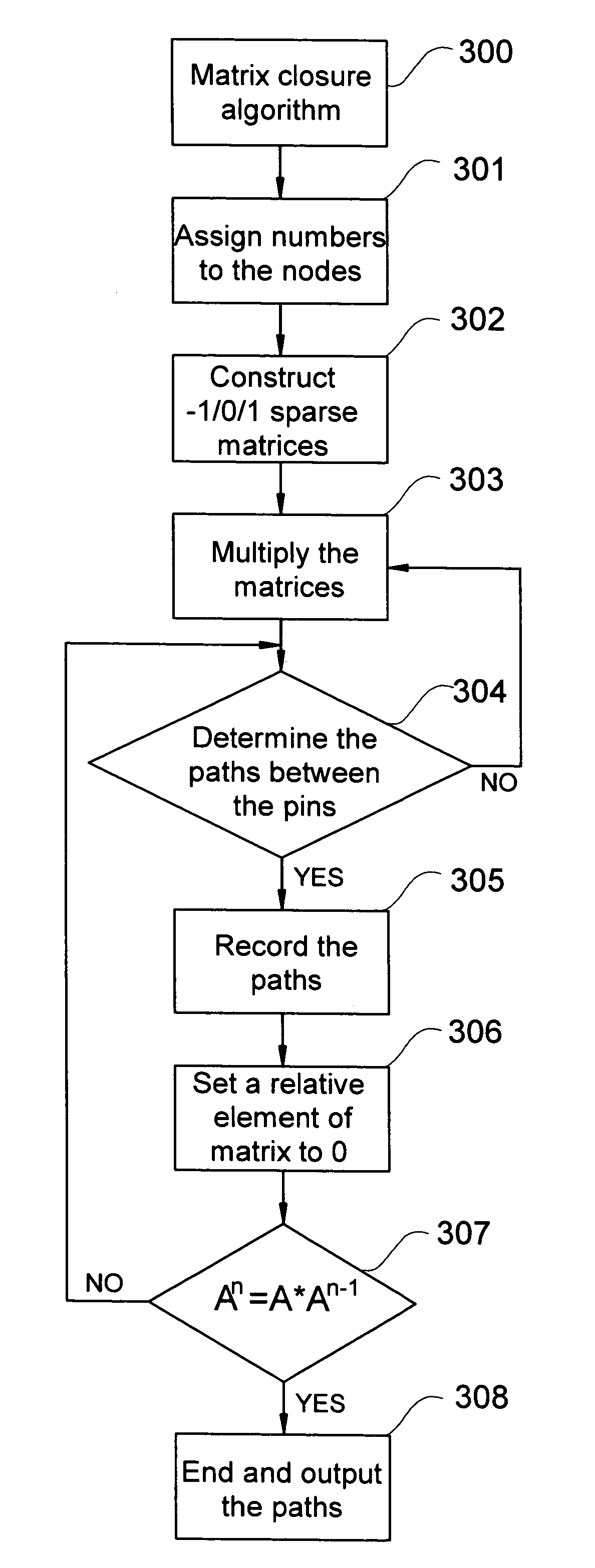
[0029]Step 3 comprises two algorithms in which step 30 involves a matrix closure algorithm and step 31 involves a supernode algorithm. For matrix closure algorithm, a −1 / 0 / 1 matrix is created by connecting nodes and a target path is obtained by multiplying matrices. For supernode algorithm in which supernodes are expanded to decrease the number of nodes, thereby reducing the complexity of searching paths that are susceptible to ESD and...


PUM


Abstract

A method of searching paths that are susceptible to electrostatic discharge (ESD) at the beginning of an integrated circuit (IC) design is disclosed that includes a circuit spreading out algorithm, a matrix closure algorithm, and a supernode algorithm. The found paths are required to satisfy conditions including that (a) they are connected from a gate of a transistor to a source or a drain thereof, and (b) the head node and the tail node of each path are pins of a top level of the IC. −1 / 0 / 1 matrix multiplication is employed by both the circuit spreading out algorithm and the matrix closure algorithm so as to obtain a result of node connections after a plurality of matrix self-multiplications.

Description

BACKGROUND OF THE INVENTION[0001]1. Field of Invention[0002]The invention relates to electrostatic discharge (ESD) prevention techniques and more particularly to a method of searching paths that are susceptible to ESD at the beginning of an integrated circuit (IC) design.[0003]2. Description of Related Art[0004]In manufacturing, assembling, packaging, and delivering of electronic devices and even at the time of using an electronic device by a user, there is pretty high probability of damaging the electronic device due to electrostatic discharge (ESD). Thus, a variety of ESD protection structures and circuits are provided and mounted in an electronic device. For example, when a deep submicron system-on-a-chip (SoC) is employed in a semiconductor manufacturing process, the SoC is susceptible to ESD. Thus, internal components of SoC may be severely damaged by momentary unwanted currents. For the protection of SoC, an ESD protection circuit is provided to eliminate ESD.[0005]ESD protect...

Claims


Application Information

Patent Timeline
Patent Type & Authority Patents(United States)
IPC IPC(8): G06F17/50
CPCG06F17/5081G06F2217/12G06F30/398G06F2119/18Y02P90/02
Inventor LAI, MING-HONGCHO, CHAO-YICHU, CHIA-CHIFENG, WU-SHIUNG
Owner CHANG GUNG UNIVERSITY
Features
  • R&D
  • Intellectual Property
  • Life Sciences
  • Materials
  • Tech Scout
  • Unparalleled Data Quality
  • Higher Quality Content
  • 60% Fewer Hallucinations
Learn More