Nitride-based semiconductor device

a technology of nitride and semiconductor, applied in the field of semiconductor devices, can solve the problems of increasing power loss, generating more heat, and nitride semiconductors on n-type silicon substrates were mostly unsatisfactory in the efficiency of light emission, so as to achieve the effect of less voltage and less voltage drop

Active Publication Date: 2008-07-15
SANKEN ELECTRIC CO LTD
View PDF9 Cites 4 Cited by
  • Summary
  • Abstract
  • Description
  • Claims
  • Application Information

AI Technical Summary

Benefits of technology

[0010]The present invention seeks, in a semiconductor device having nitride-based semiconductor regions grown on a silicon substrate, to minimize the voltage drop therebetween and to make it possible for the semiconductor device to be driven with a less voltage than heretofore.
[0013]The alloy layer functions to cause electrons and holes to be generated at its interface with the p-type silicon substrate and these electrons and holes to recombine. The result is the reduction of the potential barrier of the heterojunction between the p-type silicon substrate and the n-type buffer region. This fact, combined with the absence of a pn junction from the substrate, makes it possible to make the drive voltage of the semiconductor device drastically less than heretofore.

Problems solved by technology

The trouble, however, is that aluminum, indium and gallium diffuse deeper down into the silicon substrate from the alloy layer.
Another problem with LEDs concerns the electrodes that meet the dual, sometimes contradictory, requirements of enabling the emission of light therethrough and providing electric connections.
As the n-type silicon substrate necessitates as aforesaid the application of a high drive voltage forwardly of the LED, both silicon substrate and semiconductor region cause greater power losses and generate more heat.
The prior art LEDs having nitride semiconductors on n-type silicon substrates were therefore mostly unsatisfactory in the efficiency of light emission.
This solution is objectionable because of the additional manufacturing steps, and consequent higher manufacturing costs, needed for fabrication of the current blocking layer.

Method used


Image

  • Nitride-based semiconductor device
  • Nitride-based semiconductor device
  • Nitride-based semiconductor device

Examples


embodiment

of FIG. 4

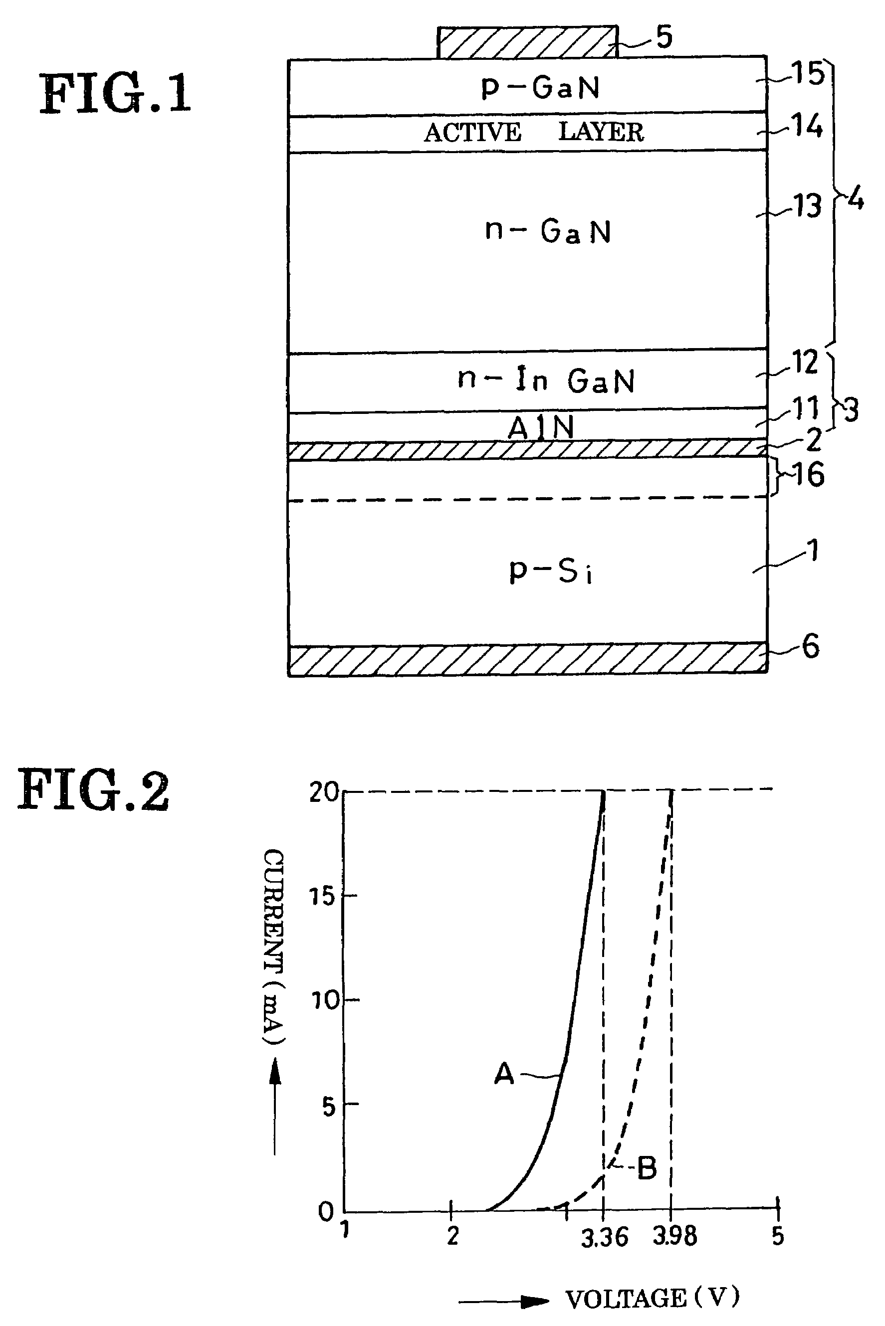
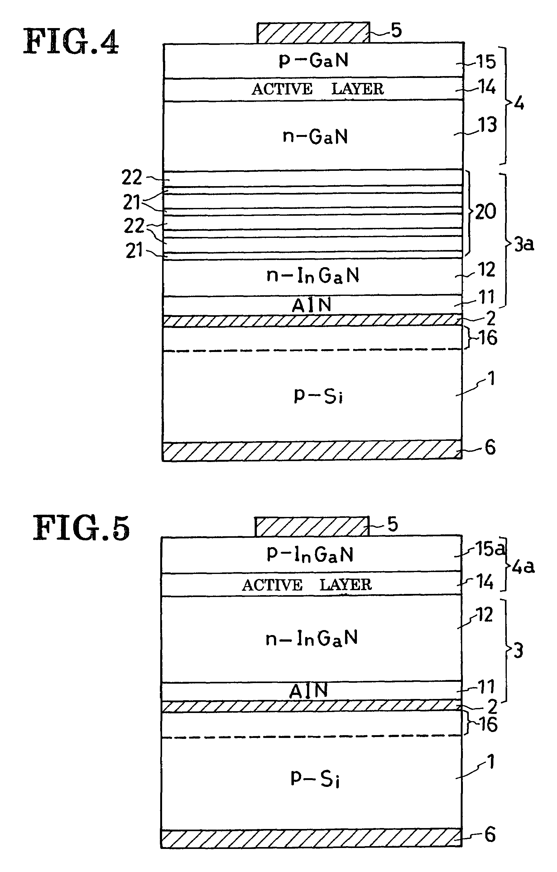
[0069]The LED shown in FIG. 4 by way of another preferred embodiment of the invention is akin to the FIG. 1 embodiment except for a modified buffer region 3a. The modification resides in a multilayered buffer subregion 20 interposed between the buffer layer 12 and the n-type nitride semiconductor layer 13 of the main semiconductor region 4. The multilayered buffer subregion 20 is an alternation of a plurality or multiplicity of first buffer sublayers 21 and a plurality or multiplicity of second buffer sublayers 22. The first buffer sublayers 21 are made from a nitride semiconductor containing a prescribed proportion of aluminum, and the second buffer sublayers 22 from a nitride semiconductor that either does not contain aluminum or does contain aluminum in a less proportion than do the first buffer sublayers 21.

[0070]The aluminum-containing nitride semiconductor materials adoptable for the first buffer sublayers 21 are generally defined as:

AlxMyGa1-x-yN

where M is at least e...


PUM


Abstract

A light-emitting diode is built on a silicon substrate doped with a p-type impurity to possess sufficient conductivity to provide a current path. The p-type silicon substrate has epitaxially grown thereon two superposed buffer layers of aluminum nitride and n-type indium gallium nitride. Further grown epitaxially on the buffer layers is the main semiconductor region of the LED which comprises a lower confining layer of n-type gallium nitride, an active layer for generating light, and an upper confining layer of p-type gallium nitride. In the course of the growth of the main semiconductor region there occurs a thermal diffusion of aluminum, gallium and indium from the buffer layers into the p-type silicon substrate, with the consequent creation of an alloy layer of the diffused metals. Representing p-type impurities in the p-type silicon substrate, these metals do not create a pn junction in the substrate which causes a forward voltage drop.

Description

CROSS REFERENCE TO RELATED APPLICATIONS[0001]This is a continuation of Application PCT / JP2004 / 007849, filed May 31, 2004, which claims priority to Japanese Patent Application No. 2003-162394 filed Jun. 6, 2003 and Japanese Patent Application No. 2004-093516 filed Mar. 26, 2004.BACKGROUND OF THE INVENTION[0002]This invention relates to semiconductor devices such as light-emitting diodes (LEDs) and transistors, particularly to those employing nitrides or nitride-based compounds as semiconductors, and to a method of making such semiconductor devices.[0003]Nitride-based semiconductor devices are capable of fabrication on substrates of either sapphire, silicon carbide, or silicon. Silicon in particular offers the advantages of being less expensive and easier of cutting than sapphire or silicon carbide. Unlike sapphire, moreover, silicon is electrically conductive and so lends itself to use as a current path. Offsetting these advantages of the silicon substrate is a relatively great volta...

Claims


Application Information

Patent Timeline
Patent Type & Authority Patents(United States)
IPC IPC(8): H01L31/0328H01L21/20H01L29/20H01L29/737H01L33/12H01L33/32H01L33/34
CPCH01L21/02381H01L21/02458H01L21/02491H01L21/02505H01L21/02507H01L21/0262H01L29/7371H01L33/12H01L21/0254H01L33/14H01L29/2003
Inventor OTSUKA, KOJISATO, JUNJIMOKU, TETSUJITADA, YOSHIKIYOSHIDA, TAKASHI
Owner SANKEN ELECTRIC CO LTD
Why Eureka
Try Eureka