Three dimensional transformer

a transformer and three-dimensional technology, applied in the direction of transformer/inductance details, fixed transformers or mutual inductances, inductances, etc., can solve the problems of increasing the cost, affecting the coupling rate, and affecting the operation of the inductor, so as to achieve the effect of enhancing the coupling ra

Active Publication Date: 2008-07-29
NATIONAL CHUNG HSING UNIVERSITY
View PDF7 Cites 35 Cited by
  • Summary
  • Abstract
  • Description
  • Claims
  • Application Information

AI Technical Summary

Benefits of technology

[0006]The present invention is to provide a three dimensional (3D) transformer in which the coupling rate is enhanced, while the chip area is preserved.

Problems solved by technology

Since a CMOS substrate is a highly consumed substrate, managing the property of the inductor is difficult.
The area of the planar structure of the GaAs circuit is large; thus, the area of the radio frequency integrated circuits becomes correspondingly large and the cost is ultimately increased.
Along with the miniaturization the micromation of devices, the traditional planar type of transformer, which occupies a large area, fails to conform to current demands.

Method used


Image

  • Three dimensional transformer
  • Three dimensional transformer
  • Three dimensional transformer

Examples


Embodiment Construction

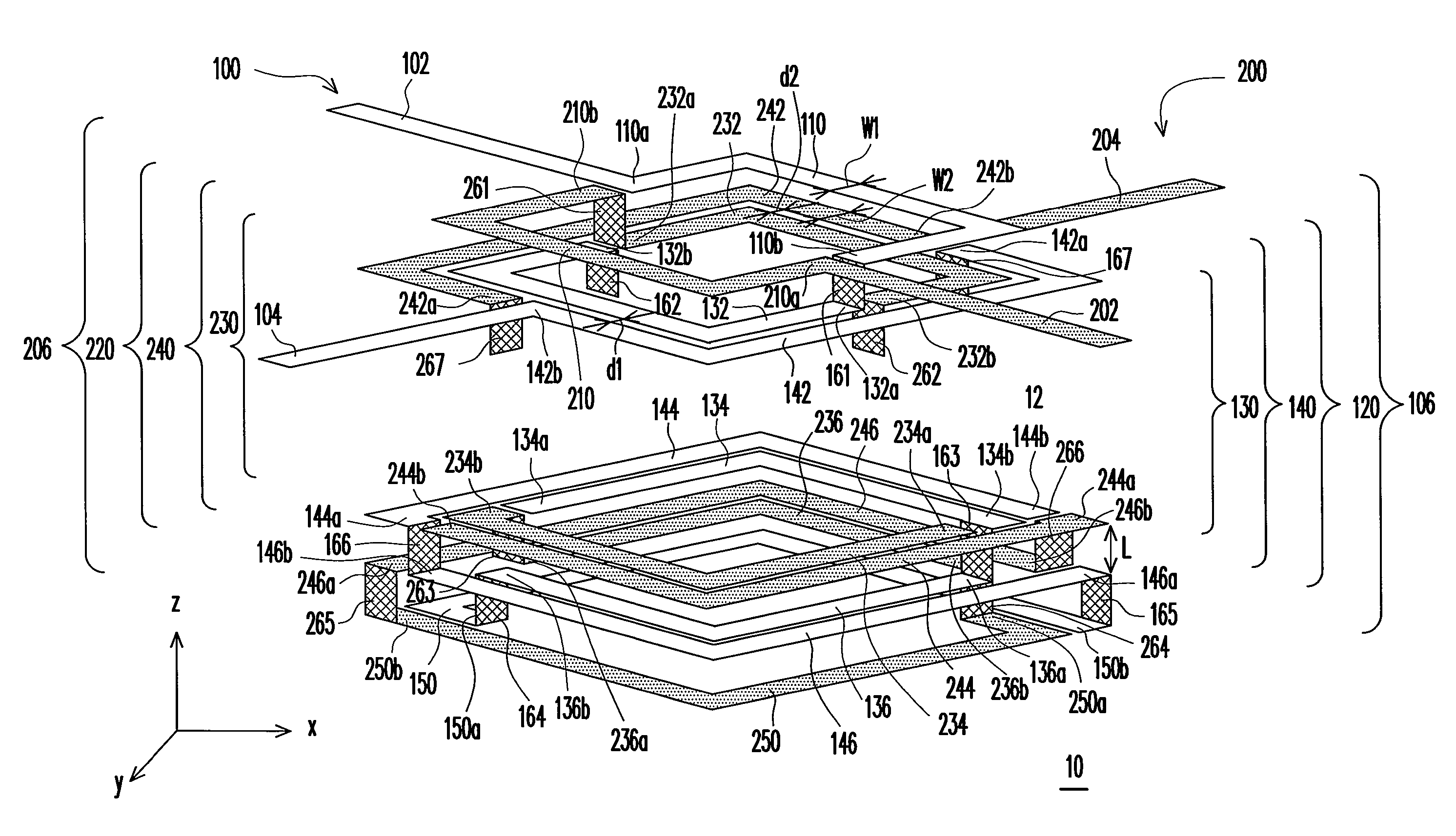
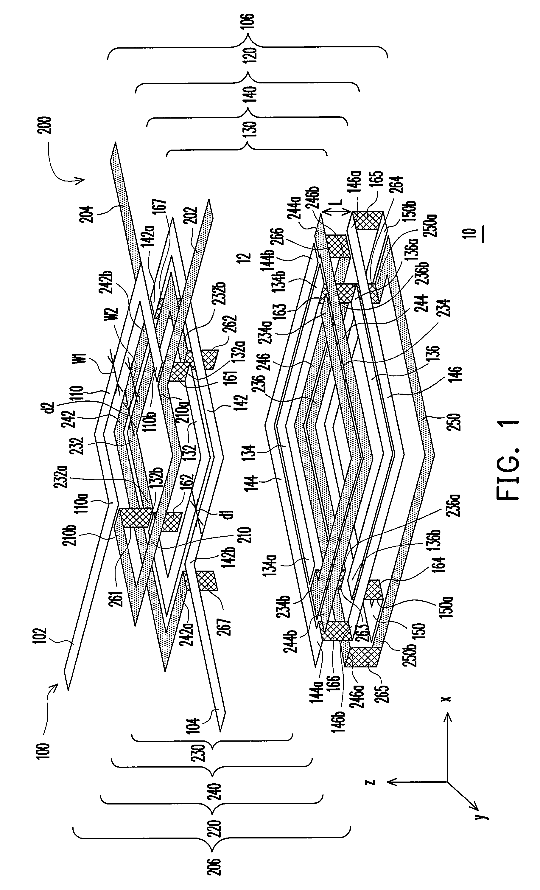
[0024]FIG. 1 is a schematic, cross-sectional view of a three dimensional (3-D) transformer according to an embodiment of the present invention. FIG. 2 is a schematic, cross-sectional view of a first coil of a three dimensional transformer according to an embodiment of the present invention. FIG. 3 is a schematic, cross-sectional view of a second coil of a three dimensional transformer according to an embodiment of the present invention.

[0025]Referring to FIG. 1, the 3-D transformer 10 of the present embodiment is disposed on a semiconductor substrate 10, wherein the 3-D transformer 10 includes a first coil 100 and a second coil 200.

[0026]Referring to FIGS. 1 and 2, the first coil 100 includes a first port 102, a second port 104 and a plurality of first metal lines 106. The plurality of the first metal lines 106 include a top layer first metal line 110, a plurality of inter-layer first metal lines 120 and a bottom layer first metal line 150. The layers of metal lines are insulated fr...


PUM

PropertyMeasurementUnit
lengthaaaaaaaaaa
widthaaaaaaaaaa
distanceaaaaaaaaaa

Abstract

A three dimensional (3D) transformer includes a first coil and a second coil. Each coil includes a first port, a second port, a top layer metal line, inter-layer inner metal lines, inter-layer outer metal lines and a bottom layer metal line. Each metal line of the first coil and that of the second coil are correspondingly arranged to the opposite side of each other. Each of the first port is electrically connected to each of the top metal line. Each coil is arranged clockwise from the top metal line, the inter layer inner metal line down to the bottom layer metal line and arranged clockwise from the bottom layer metal line, the inter layer outer metal line up to the upper metal line of the inter layer outer metal line. Each upper metal line of the inter layer outer metal line is electrically connected to each second port.

Description

BACKGROUND OF THE INVENTION[0001]1. Field of Invention[0002]The present invention relates to a radio frequency integrated circuits. More particularly, the present invention relates to a three dimensional (3D) transformer.[0003]2. Description of Related Art[0004]In recent years, the demand for radio frequency integrated circuits has increased significantly due the popularity and convenience of wireless communication. In the design of complementary metal oxide semiconductor (CMOS) radio frequency integrated circuits, the inductor is a very important device to be considered asides from controlling the high frequency property of the active device. Since a CMOS substrate is a highly consumed substrate, managing the property of the inductor is difficult. In the conventional CMOS radio frequency integrated circuits, the inductor is configured on the planar structure of the GaAs circuit. The area of the planar structure of the GaAs circuit is large; thus, the area of the radio frequency int...

Claims


Application Information

Patent Timeline
Patent Type & Authority Patents(United States)
IPC IPC(8): H01F5/00
CPCH01F27/2804H01F17/0013H01F2027/2819H01F19/04
Inventor HSU, HENG-MINGHUANG, KUO-HSUN
Owner NATIONAL CHUNG HSING UNIVERSITY
Why Eureka
Try Eureka