Liquid crystal display device

a liquid crystal display and active matrix technology, applied in non-linear optics, instruments, optics, etc., can solve the problems of limited thickness or material of wires on the edge of tft substrates, difficult to use low-resistance materials such as copper, and process-related limitations, so as to reduce wiring resistance and prevent color unevenness , good display quality

Inactive Publication Date: 2008-08-19
SHARP KK
View PDF7 Cites 15 Cited by
  • Summary
  • Abstract
  • Description
  • Claims
  • Application Information

AI Technical Summary

Benefits of technology

[0017]It is therefore an object of the invention to provide a liquid crystal display device which is capable of preventing unevenness in color or brightness resulting from wiring resistance between an input part and driver boards and between the driver boards, thereby achieving good display quality, even when a panel is of a larger size.
[0019]Therefore, in the liquid crystal display device of the invention, the wiring board having the wiring disposed thereon is bonded to the edge of the one substrate in the region between the driver boards, and the wiring serves to provide electrical connection between two adjacent driver boards. A general flexible printed wiring board, which is formed of a resin film, such as polyimide, and copper foil bonded to the resin film, may be used as the wiring board. As described above, the wiring board is bonded in the region between two driver boards, and the wiring on the wiring board provides electrical connection between the two driver boards. Thus, the liquid crystal display device of the invention enables a sufficiently substantial reduction in wiring resistance. Accordingly, the liquid crystal display device of the invention can prevent unevenness in color or brightness resulting from a voltage drop due to wiring resistance, and thereby achieving good display quality.

Problems solved by technology

Thus, the wiring on the edge of the TFT substrate is limited in thickness or material, and it is therefore difficult to use a low-resistance material, such as copper.
The wiring is also limited in width in terms of process, and it is thus difficult to form the wiring having such a great width that wiring resistance is negligible.

Method used


Image

  • Liquid crystal display device
  • Liquid crystal display device
  • Liquid crystal display device

Examples


Embodiment Construction

[0024]An embodiment of the invention will be described below with reference to the accompanying drawings.

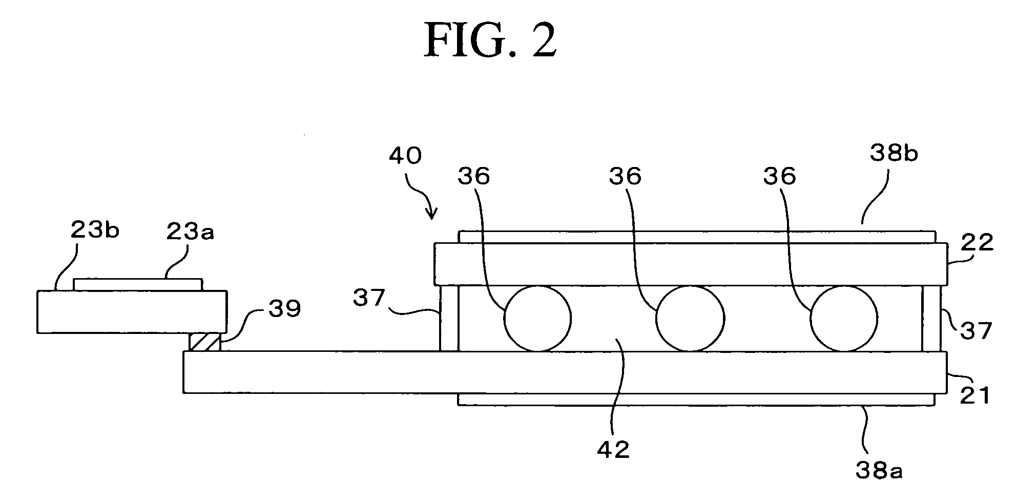
[0025]FIG. 2 is a schematic cross-sectional view showing a liquid crystal display device. according to the embodiment of the invention. Incidentally, the description is given with regard to the embodiment of the invention as applied to a transmissive liquid crystal display device.

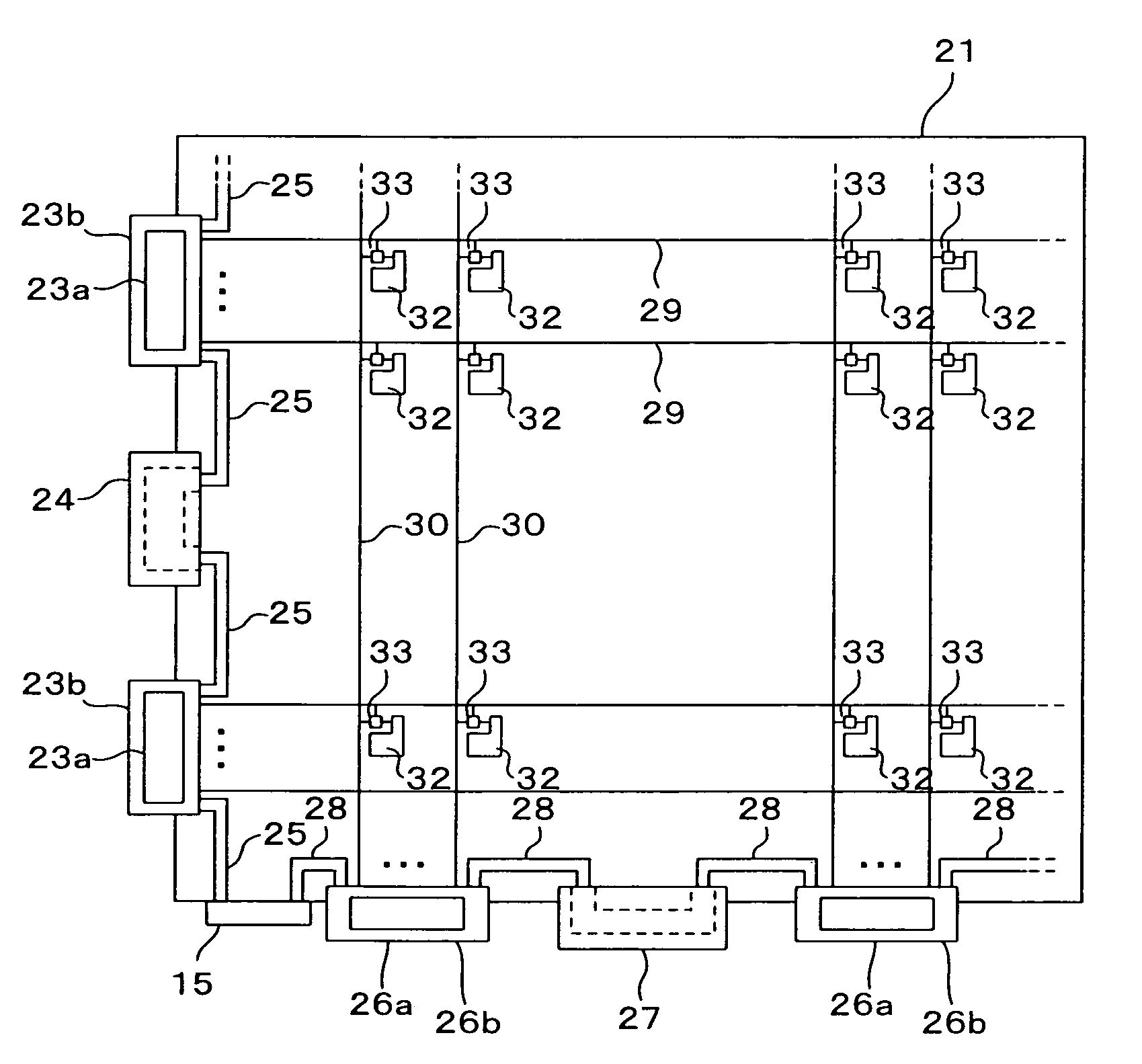
[0026]A liquid crystal panel 40 comprises a TFT substrate 21 and an opposite substrate 22 which are disposed with spacers 36 in between and are bonded with a sealing compound 37, and liquid crystal 42 sealed in between the TFT substrate 21 and the opposite substrate 22. The TFT substrate 21 is slightly larger than the opposite substrate 22 and partly extends beyond the opposite substrate 22. Gate driver boards 23b each having a gate driver 23a mounted thereon, and other components are connected to the extending part of the TFT substrate 21 by the use of ACFs 39 (anisotropic conductive films), as will be ...


PUM

PropertyMeasurementUnit
voltageaaaaaaaaaa
voltageaaaaaaaaaa
voltageaaaaaaaaaa

Abstract

A plurality of gate driver boards are bonded to a first side of a TFT substrate, and a wiring board made of a flexible printed wiring board is bonded between the gate driver boards. Then, a wiring disposed on the wiring board provides connection between adjacent gate driver boards. In the same manner, a plurality of data driver boards are bonded to a second side of the TFT substrate, and a wiring board made of a flexible printed wiring board is bonded between the data driver boards. Then, a wiring disposed on the wiring board provides connection between adjacent data driver boards.

Description

CROSS-REFERENCE TO RELATED APPLICATIONS[0001]This application is based on and claims priority of Japanese Patent Application No. 2004-282416 filed on Sep. 28, 2004, the entire contents of which are being incorporated herein by reference.BACKGROUND OF THE INVENTION[0002]1. Field of the Invention[0003]The invention relates to an active matrix liquid crystal display device and more particularly to a liquid crystal display device suitable for a larger screen.[0004]2. Description of the Prior Art[0005]Liquid crystal display devices have the advantages of being thin and lightweight and also allowing low-voltage drive and thus low power consumption. Thus, liquid crystal display devices are used in various types of electronic equipment, such as televisions, PCs (personal computers), PDAs (personal digital assistants), and mobile telephones. In particular, an active matrix liquid crystal display device, which includes a TFT (thin film transistor) which is provided for each picture element (o...

Claims


Application Information

Patent Timeline
Patent Type & Authority Patents(United States)
IPC IPC(8): G02F1/1345
CPCG02F1/13452G02F1/1345G02F1/133
Inventor FURUKOSHI, YASUTAKE
Owner SHARP KK
Why Eureka
Try Eureka