Semiconductor device, display device, and electronic device

a display device and semiconductor technology, applied in the direction of logic circuit coupling/interface arrangement, pulse technique, instruments, etc., can solve the problems of terminal out malfunction, distortion of signal waveform, and malfunction, so as to minimize the load on the input terminal, the effect of reducing the load and ensuring stability

Inactive Publication Date: 2008-10-07
SEMICON ENERGY LAB CO LTD
View PDF12 Cites 41 Cited by
  • Summary
  • Abstract
  • Description
  • Claims
  • Application Information

AI Technical Summary

Benefits of technology

[0012]However, in the configurations shown in FIGS. 38A and 38B, in the non-selection period, the terminal OUT1 and terminals OUTx in the following stages are floated. Therefore, there is a problem in that a terminal OUT malfunctions due to noise generated by the clock signal 1 and the clock signal 2, or noise caused by an electromagnetic wave from outside the circuit. Further, since a capacitor element is provided between an electrode connected to a gate electrode of the transistor for resetting terminals Px in each stage and the input terminal Vin in the configuration shown in FIGS. 38A and 38B; a load for driving the input terminal Vin is heavy. Therefore, there are also the problems of distortion of waveforms of signals and heavy power consumption. Since the transistor for resetting the terminals Px in each stage is ON during most of the non-selection period, there is also a problem in that voltage stress is heavily biased on the gate electrode and characteristics vary easily.
[0047]Further, when the average of the gate area of a third transistor and the gate area of a second transistor is made larger than the gate area of a first transistor, since it is not necessary to connect a capacitor element to an input terminal, load on the input terminal can be minimized. Thus, a semiconductor device with little waveform distortion and low power consumption; a display device including the semiconductor device; and an electronic device including the display device can be provided.

Problems solved by technology

Accordingly, there has been a problem in that malfunction is caused due to noise generated by a clock signal 1 and a clock signal 2 or noise caused by an electromagnetic wave from outside the circuit.
Therefore, there is a problem in that a terminal OUT malfunctions due to noise generated by the clock signal 1 and the clock signal 2, or noise caused by an electromagnetic wave from outside the circuit.
Therefore, there are also the problems of distortion of waveforms of signals and heavy power consumption.
Since the transistor for resetting the terminals Px in each stage is ON during most of the non-selection period, there is also a problem in that voltage stress is heavily biased on the gate electrode and characteristics vary easily.

Method used


Image

  • Semiconductor device, display device, and electronic device
  • Semiconductor device, display device, and electronic device
  • Semiconductor device, display device, and electronic device

Examples


embodiment modes

[0087]Embodiment Modes of the present invention will be described with reference to the drawings. Note that the present invention can be embodied with many different modes, and it is easily understood by those skilled in the art that the modes and details can be variously modified without departing from the spirit and scope of the present invention. Therefore, the present invention should not be construed as being limited to the description of the Embodiment Modes. In the structures of the invention described hereinafter, the same reference numerals are given to the same parts or parts having similar functions in different drawings, and the description of such parts will not be repeated.

embodiment mode 1

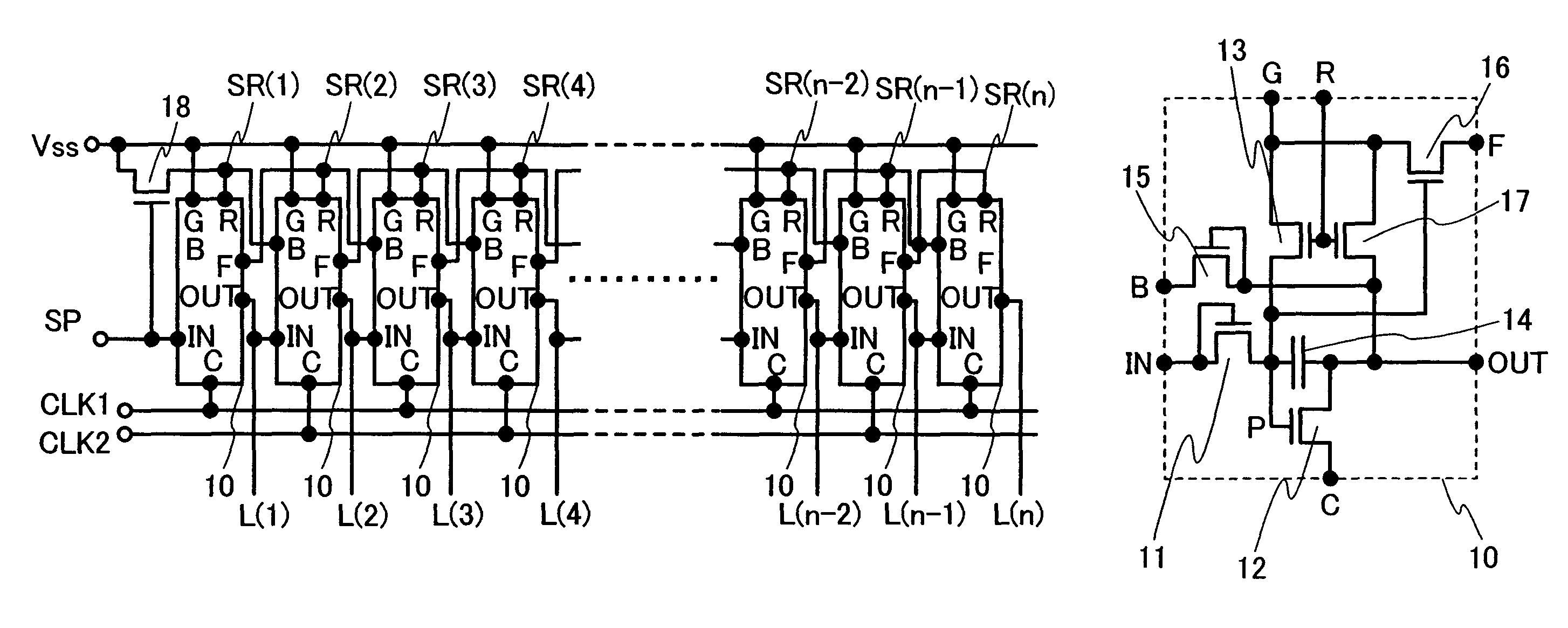
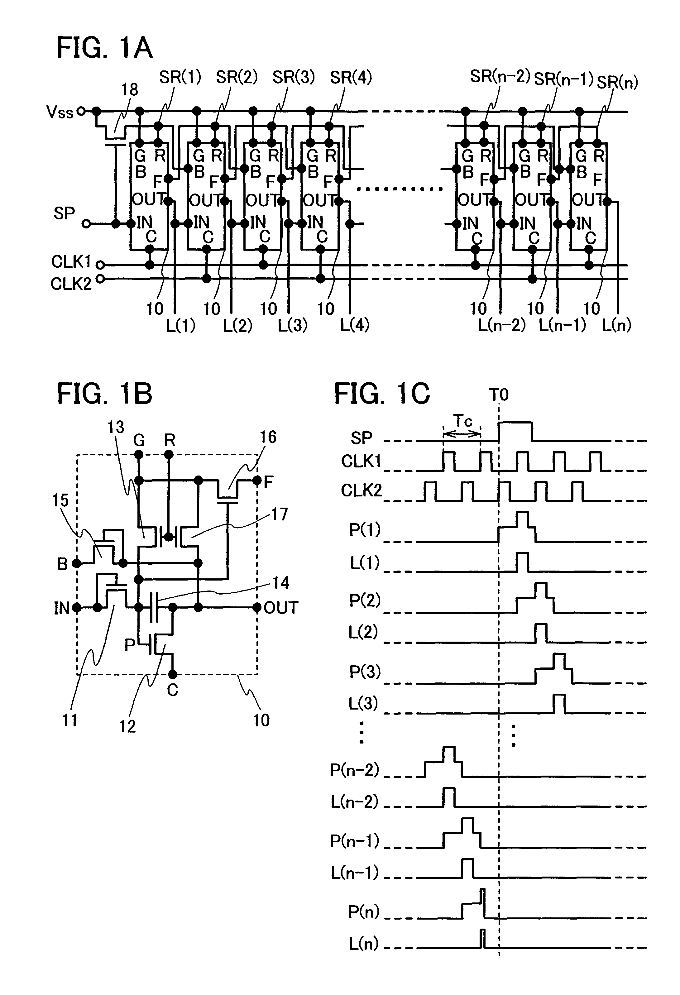
[0088]In this embodiment mode, a circuit configuration of a shift register where the electric potential of an output terminal is fixed to a non-selection period, thereby reducing the occurrence of malfunctions due to clock signals or noise, will be described. Circuit configuration examples of a shift register of the present invention are shown in FIGS. 1A to 1C. FIG. 1A shows the entire circuit configuration of a shift register circuit of the present invention. FIG. 1B shows a configuration example of a circuit 10 which shows a single stage circuit of a shift register of the present invention. Note that in this specification, a single stage circuit refers to a minimum unit for forming a circuit, which corresponds to an output terminal (L(1) to L(n)) of the circuit, as does FIG. 1B with respect to FIG. 1A. FIG. 1C shows waveforms of an input signal, an internal electrode, and an output signal in the circuit shown in FIGS. 1A and 1B.

[0089]The circuit shown in FIG. 1A is provided with ...

embodiment mode 2

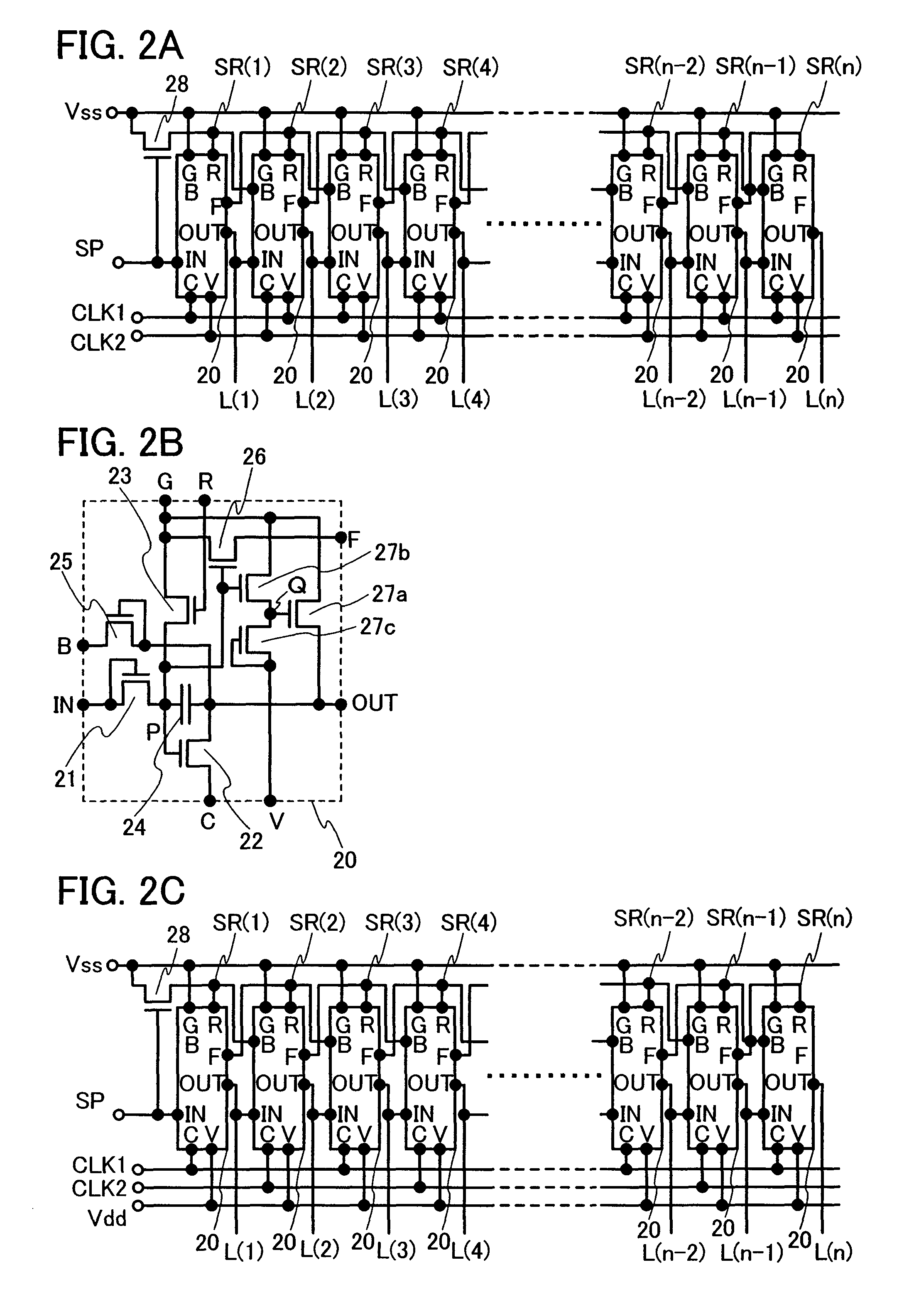
[0153]In this embodiment mode, reset operation of the last stage and the reset operation of all the stages of the shift register circuit of the present invention will be described.

[0154]In the circuit configuration described in Embodiment Mode 1, the reset operation of the current stage is conducted at the timing of the operation of the next stage. Here, since there is no stage after the shift register circuit at the last stage, no pulse defining the timing of the reset operation is inputted to the last stage. Therefore, the electric potential of the electrode SR(n) will not be at H level by reset operation. Accordingly, clock signals are constantly outputted to the terminal OUT of the last stage.

[0155]Considering the points, in Embodiment Mode 1, the electrode SR(n) is connected to the electrode SR(n−1) as shown in FIG. 1A, FIG. 2A, and FIG. 2C. Thus, reset operation can be performed by making the electrode SR(n) at H level with the output of the terminal OUT at the last stage itse...


PUM


Abstract

To provide a semiconductor device which operates stably with few malfunctions due to noise, with low power consumption, and little variation in characteristics; a display device including the semiconductor device; and an electronic device including the display device. An output terminal is connected to a power supply line, thereby reducing variation in electric potential of the output terminal. In addition, a gate electrode potential which turns ON a transistor is maintained due to the capacitance of the transistor. Further, change in characteristics of the transistor is reduced by a signal line for reverse bias.

Description

BACKGROUND OF THE INVENTION[0001]1. Field of the Invention[0002]The present invention relates to a semiconductor device, a display device, and an electronic device.[0003]2. Description of the Related Art[0004]A shift register circuit is a circuit which operates such that content thereof is shifted by one stage each time a pulse is applied. Utilizing this property, shift registers are used in circuits for mutual conversion of serial signals and parallel signals. Such circuits which convert serial signals to parallel signals, or convert parallel signals to serial signals are mainly used for networks having circuits connected to each other. The number of transmission paths for connecting circuits to each other and transmitting signals in a network is often small relative to the amount of data to be transmitted. In such cases, parallel signals are converted into serial signals in a transmitter circuit and are sequentially sent to a transmission path, and serial signals that have been se...

Claims


Application Information

Patent Timeline
Patent Type & Authority Patents(United States)
IPC IPC(8): G09G3/36G06F7/38
CPCG09G3/2096G09G3/3648G11C19/28G09G2310/0275G09G2330/021G09G2310/0267G09G3/20G09G2310/0286H01L2924/10253G11C7/10G11C7/22G09G3/3688G09G3/3677G09G2300/0426G09G2310/08
Inventor YOSHIDA, YASUNORI
Owner SEMICON ENERGY LAB CO LTD
Why Eureka
Try Eureka