Fast microbolometer pixels with integrated micro-optical focusing elements

a technology of optical focus elements and micro-bolometers, applied in the field of fast micro-bolometer pixels, can solve the problems of poor thermal resolution, small improvement in performance, and inability to justify the introduction of additional optical elements, and achieve the effect of increasing the thermal mass

Active Publication Date: 2008-10-21
INSTITUT NATIONAL D'OPTIQUE
View PDF20 Cites 3 Cited by
  • Summary
  • Abstract
  • Description
  • Claims
  • Application Information

AI Technical Summary

Benefits of technology

[0005]It is thus an object of the present invention to provide fast microbolometer pixels with integrated micro-optical focusing elements, where no additional structures attached to the detector which would otherwise increase the thermal mass are required.

Problems solved by technology

Smaller detectors are therefore faster, but because the radiation absorbed by the detector is proportional to its surface area, the speed of smaller detectors comes at the price of poorer thermal resolution.
The modest improvement in performance possible does not justify the introduction of an additional optical element for standard microbolometer focal planes in video rate imaging applications.
The cost of large and even ‘small’ satellite platforms being very great, these missions are now typically planned for micro or even nano-satellite platforms.
However, in contrast to cooled photonic detectors, uncooled detectors respond very slowly to incoming radiation, and even recent ‘fast’ microbolometer pixels are too slow to resolve ground spots below about 250 m for a low earth orbit satellite.
Many missions require 50 or 100 m ground spots, so there is a great unmet need for faster uncooled detectors.
The same considerations apply to linear uncooled arrays for industrial and commercial applications, where the response time of the detectors limits the achievable data acquisition rates.

Method used


Image

  • Fast microbolometer pixels with integrated micro-optical focusing elements
  • Fast microbolometer pixels with integrated micro-optical focusing elements
  • Fast microbolometer pixels with integrated micro-optical focusing elements

Examples


Embodiment Construction

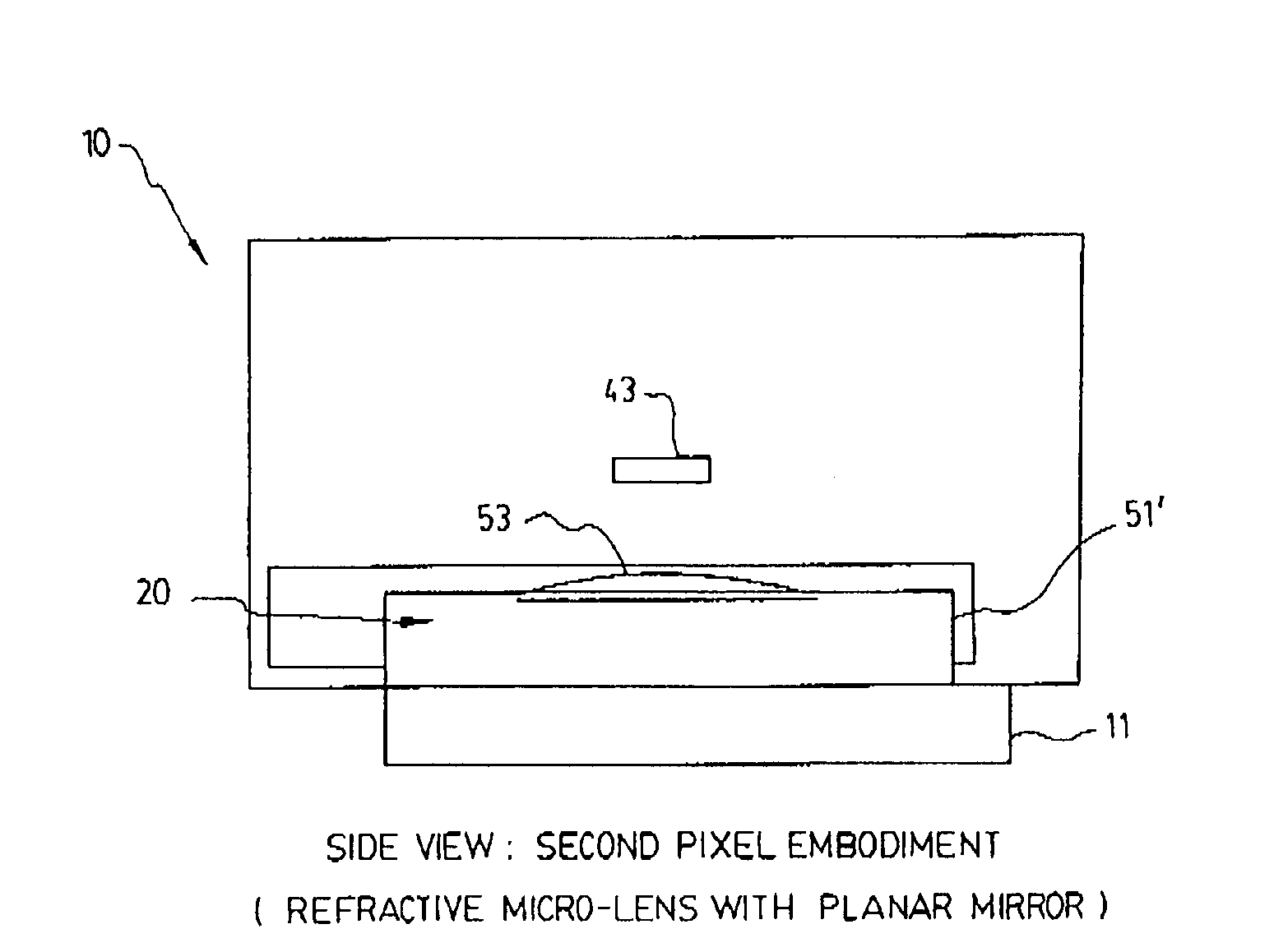
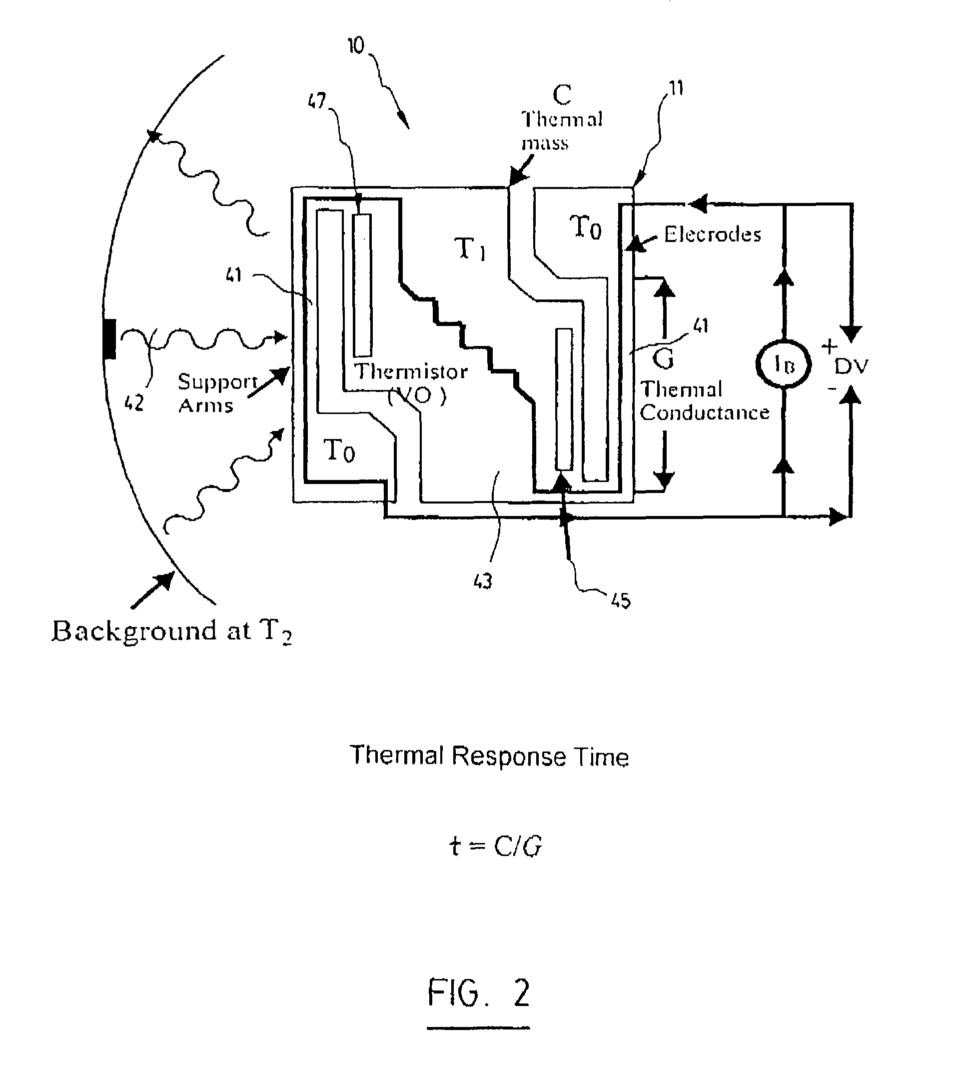
[0016]The present invention is directed to fast microbolometers that are intentionally built smaller than the detector unit cell to increase pixel speed and provided with some form of focusing element to improve the thermal resolution of the microbolometer, and of the resulting array.

[0017]In this case, it has been found that a microoptics / detector combination is the preferred way to collect the required incident radiation without using an additional structure attached to the detector (such as an antenna) that would in turn increase the thermal mass. As an alternative to the use of a separate microlens array, it is preferable to implement monolithically an array of parabolic mirrors underneath the detectors themselves. This approach has the additional advantage of eliminating alignment concerns and simplifying packaging, at the expense of a more complicated fabrication process flow. A standard detector with 50 μm pitch has a central portion area on the order of 1600 μm2. If a detect...


PUM


Abstract

Fast microbolometer pixels integrating micro-optical focusing elements are provided. Each microbolometer pixel includes a focusing element located between the pixel body and a substrate, this focusing element preferably sending radiation back towards the central portion of the microbolometer. There is also provided a microbolometer array having a plurality of such microbolometer pixels. Advantageously, to increase the pixel speed, the present microbolometers may be built smaller than the detector and no additional structures need to be attached to said detector.

Description

FIELD OF THE INVENTION[0001]The present invention relates to fast microbolometer pixels which are provided with integrated micro-optical focusing elements.DESCRIPTION OF THE PRIOR ART[0002]Microbolometers are now quite common and are more and more used in the imaging field. These detectors are adapted to detect infrared radiation, and can be cooled or uncooled.[0003]The speed of a bolometer detector is proportional to its thermal mass divided by its thermal conductance. Smaller detectors are therefore faster, but because the radiation absorbed by the detector is proportional to its surface area, the speed of smaller detectors comes at the price of poorer thermal resolution. A non-contact means of concentrating incident radiation in a detector unit cell onto a detector that is itself much smaller than the unit cell would provide speed advantages without the penalty of reduced absorption. In the past, it has been proposed to combine arrays of microlenses with detector arrays to improv...

Claims


Application Information

Patent Timeline
Patent Type & Authority Patents(United States)
IPC IPC(8): G01J5/02
CPCG01J5/08G01J5/0806G01J5/0809G01J5/0815G01J5/20G01J2005/0077G01J5/0808
Inventor POPE, TIMOTHYTREMBLAY, BRUNOPICARD, FRANCIS
Owner INSTITUT NATIONAL D'OPTIQUE
Why Eureka
Try Eureka