Floating body cell (FBC) memory device with a sense amplifier for refreshing dummy cells
a floating body cell and memory device technology, applied in semiconductor devices, digital storage, instruments, etc., can solve the problems of difficult to further reduce the size of the fbc memory device, large memory area,
- Summary
- Abstract
- Description
- Claims
- Application Information
AI Technical Summary
Problems solved by technology
Method used
Image
Examples
first embodiment
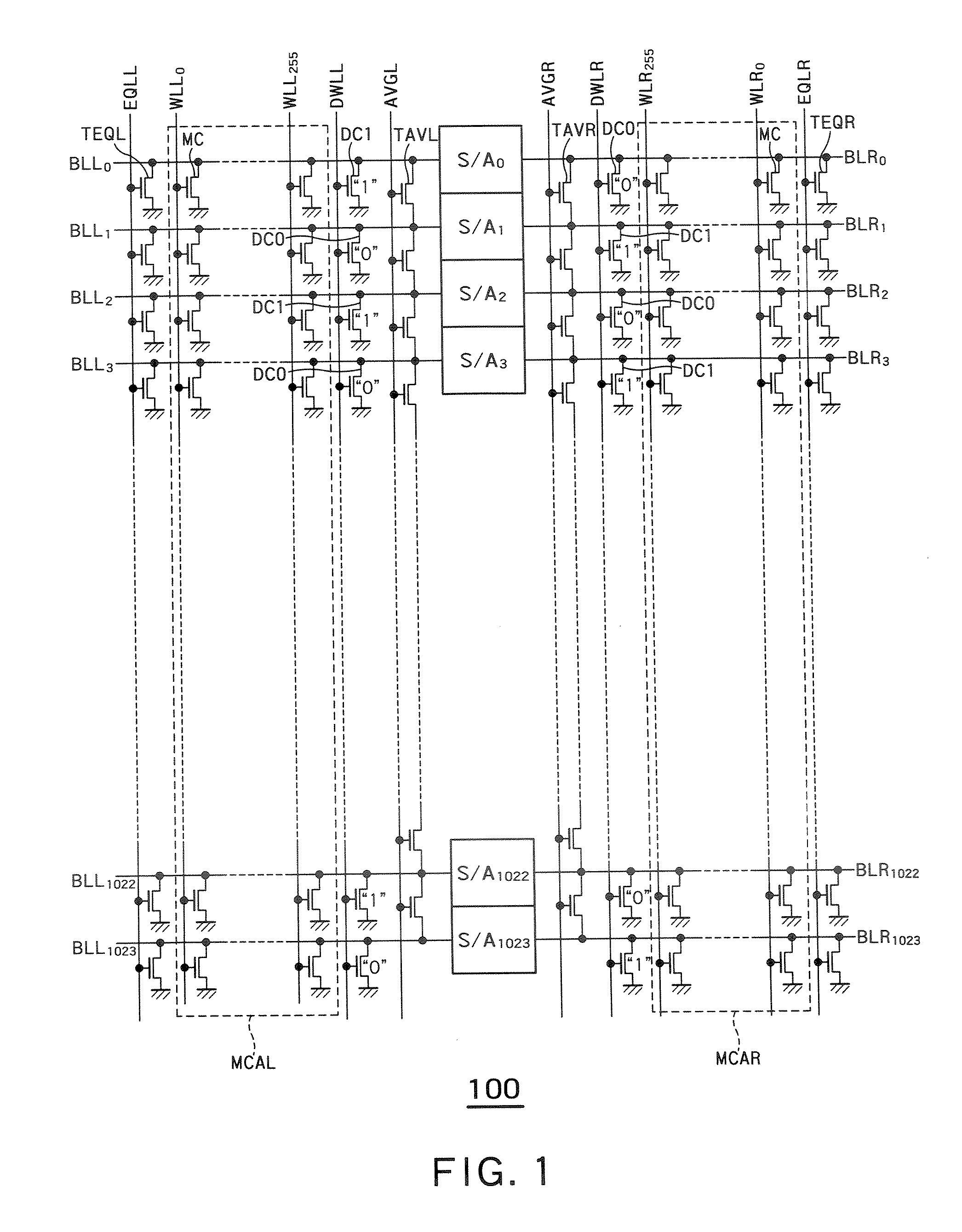
[0033]FIG. 1 is a schematic circuit diagram of an FBC memory device 100 according to an embodiment of the present invention. The FBC memory device 100 includes memory cells MCs, a dummy cell DC0 as a first dummy cell, a dummy cell DC1 as a second dummy cell, word lines WLLi, WLRi (i is an integer) (hereinafter, also “WL”), dummy word lines DWLL, DWLR (hereinafter, also “DWL”), bit lines BLL1, BLRi (hereinafter, also “BL”), sense amplifiers S / Ai (hereinafter, also “S / A”), equalizing lines EQLL, EQLR (hereinafter, also as “EQL”) equalizing transistors TEQL, TEQR (hereinafter, also as “TEQ”), averaging lines AVGL, AVGR (hereinafter, also as “AVG”), and averaging transistors TAVL, TAVR (hereinafter, also as “TAV”).
[0034]The memory cells MCs are arranged in matrix, and constitute memory cell arrays MCAL, MCAR (hereinafter, also “MCA”). The word line WL is extended in a row direction, and is connected to a gate of the memory cell MC. The word lines WLs are provided by 256 lines at each of...
second embodiment
[0128]In a second embodiment, a potential asymmetry is given to sense node pairs, by applying a potential of a predetermined polarity to the sense nodes. As a result, data of a predetermined polarity can be simultaneously written into the dummy cell pairs, or the dummy cells can be refreshed.
[0129]FIG. 20 is a circuit diagram of a sense amplifier S / A according to the second embodiment of the present invention. A total configuration of the device is similar to that shown in FIG. 1. In the second embodiment, the sense amplifier S / A receives signals of two systems of signals Φt1 and Φt0 to control the transfer gates TGL1, TGR1. The signal Φt0 is used in the transfer gate TGL1 of an even sense amplifier S / Ai (i=2x), and in the transfer gate TGR1 of an odd sense amplifier S / Ai (i=2x+1). The signal Φt1 is used in the transfer gate TGL1 of an odd sense amplifier S / Ai (i=2x+1), and in the transfer gate TGR1 of an even sense amplifier S / Ai (i=2x). The signals Φt1 and Φt0 are used to control ...
PUM
 Abstract
Description
Claims
Application Information


