Computer-readable recording medium storing semiconductor designing program for improving both integration and connection of via-contact and metal

a computer-readable and program-based technology, applied in the field of semiconductor devices, can solve the problems of deteriorating the integration of metal wires, small circuit patterns with problems, optical proximity effect, etc., and achieve the effect of minimizing contact defects and high integration

Inactive Publication Date: 2008-10-28
KK TOSHIBA
View PDF32 Cites 8 Cited by
  • Summary
  • Abstract
  • Description
  • Claims
  • Application Information

AI Technical Summary

Benefits of technology

[0011]An object of the present invention is to provide a semiconductor device that is highly integrated and minimizes contact defects between metal wires and vials, a method of designing such a semiconductor device, and a recording medium storing a program for designing such a semiconductor device.
[0012]Another object of the present invention is to provide a semiconductor device involving a short development time, a method of designing such a semiconductor device, and a recording medium storing a program for designing such a semiconductor device.
[0015]According to the first aspect, the extension is extended in line with the main wire from an end of the main wire beyond the via-contact with the width of the extension being equal to or narrower than the width of the main wire. The optical proximity effect rounds only an end of the extension, and therefore, the end of the main wire is intact and is properly connected to the via-contact without bulging around the via-contact. As a result, other main wires or via-contacts may be arranged on grid lines or on grid intersections in the vicinity of the via-contact in question without violating design rules. This realizes a highly integrated layout for a semiconductor device with densely arranged wires and via-contacts.
[0023]According to the third aspect, each via-contact has extensions each connected to an end of a main wire. The optical proximity effect rounds only the extensions, and therefore, the end of each main wires is intact and is properly connected to the via-contact. An end of each main wire is not widened around a via-contact, so that other main wires or via-contacts may be arranged on grid lines or on grid intersections in the vicinity of the via-contact in question without violating design rules. This realizes a highly integrated layout for a semiconductor device with densely arranged wires and via-contacts. Data for via-contacts entered into an automatic layout tool may include data for the extensions, so that there is no necessity to provide a main wire with the extension as a supplementary fringe when preparing data to make a mask. This decreases the quantity of design pattern data, shortens a mask data preparation time, and reduces a semiconductor device development time.
[0028]According to the fourth aspect, each via-contact has extensions each connected to an end of a main wire. The optical proximity effect rounds only the extensions, and therefore, the end of each main wire is intact and is properly connected to the via-contact. Data for via-contacts entered into an automatic layout tool may include data for the extensions, so that there is no necessity to provide a main wire with the extension as a supplementary fringe when preparing data to make a mask. This decreases the quantity of design pattern data, shortens a mask data preparation time, and reduces a semiconductor device development time.

Problems solved by technology

The very small circuit patterns have a problem.
The problem is an optical proximity-effect that occurs during a lithography process even if masks or steppers for producing circuit patterns are precise.
If the rounded wire end is connected to a via-contact, it reduces or eliminates a contact area between the wire end and the via-contact, to increases contact resistance between the wire and the via-contact and cause an open defect.
These conditions deteriorate the integration of metal wires in a semiconductor device.

Method used


Image

  • Computer-readable recording medium storing semiconductor designing program for improving both integration and connection of via-contact and metal
  • Computer-readable recording medium storing semiconductor designing program for improving both integration and connection of via-contact and metal
  • Computer-readable recording medium storing semiconductor designing program for improving both integration and connection of via-contact and metal

Examples


first embodiment

[0056]FIG. 5 is plan view showing metal wires of a semiconductor device according to the first embodiment of the present invention. The semiconductor device has via-contacts 1 and 2, main wires 3 to 6, and extensions 7 to 10. An end of each main wire is connected to a corresponding via-contact. Each extension is in line with a corresponding main wire, is connected to an end of the main wire, and is extended beyond the via-contact to which the main wire is connected. The width of each extension is equal to or narrower than the width of the corresponding main wire.

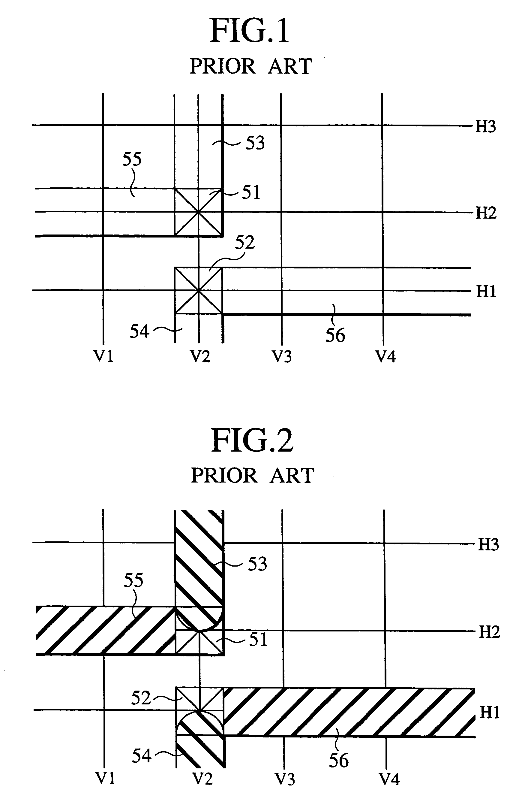
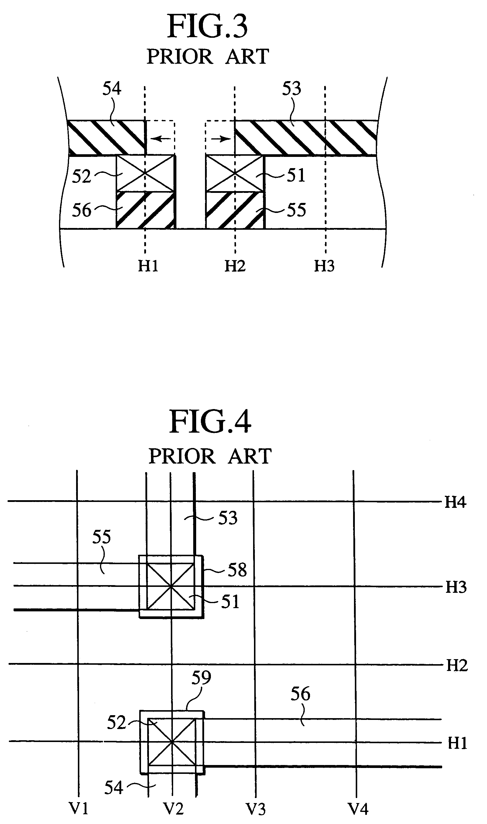
[0057]Via-contacts are conductive plugs formed in an intermediate layer between wiring layers in a semiconductor device of multilayer wiring struggle, to electrically connect metal wires formed on the upper and lower wiring layers to each other. In FIG. 5, the via-contacts 1 and 2 are arranged on a grid that is used for a designing purpose. The distance between adjacent grid lines indicates a minimum distance by which adjace...

second embodiment

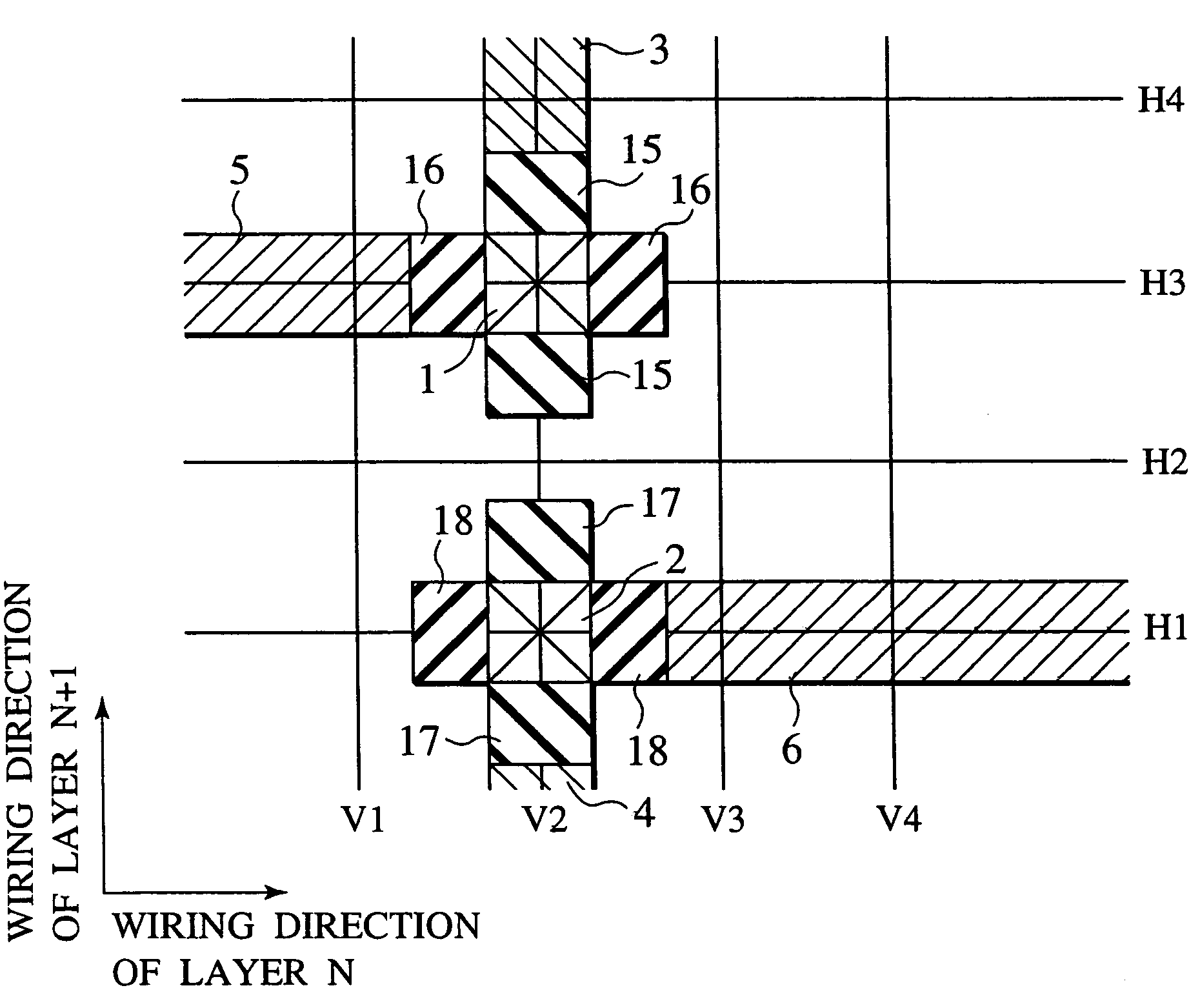
[0081]Unlike the first embodiment that ranges extensions in line with main wires, the second embodiment arranges extensions orthogonally to main wires. FIG. 12 is a plan view showing metal wires of a semiconductor device according to the second embodiment.

[0082]The semiconductor device of the second embodiment has X wiring layers where “X” is a natural number and “N” is any natal number that satisfies 01, 2), main wires (3 to 6) having ends connected to the via-contacts, and extension (15 to 18) orthogonally extending from the ends of the main wires beyond the via-contacts, the width of each extension being equal to or narrower than the width of a corresponding main wire.

[0083]The via-contacts 1 and 2 are formed in a layer N of the semiconductor device, the main wires 3 and 4 are formed in a layer N+1, and the main wires 5 and 6 are formed in the layer N. The via-contacts 1 and 2 and main wires 3 to 6 are the same as those of the first embodiment, and therefore, will not be explaine...


PUM

PropertyMeasurementUnit
widthaaaaaaaaaa
contact resistanceaaaaaaaaaa
distanceaaaaaaaaaa

Abstract

A semiconductor device has a via-contact, a main wire having an end connected to the via-contact, and an extension extended in line with the main wire from the end of the main wire beyond the via-contact, the width of the extension being equal to or narrower than the width of the main wire. The extension prevents the end of the main wire from being rounded by an optical proximity effect, eliminates a contact defect or an open defect between the via-contact and the end of the main wire, and involves no widening of the main wire around the via-contact, so that other via-contacts may be arranged in the vicinity of the via-contact in question without violating design rules.

Description

[0001]This is a division of U.S. patent application No. 10 / 675,957, filed Oct. 2, 2003, now U.S. Pat. No. 6,826,742 which is a divisional application of which is a divisional application of U.S. patent application No. 09 / 658,452, filed Sep. 8, 2000 (now U.S. Pat. No. 6,753,611,issued Jun. 22, 2004), all of which are incorporated herein by reference.BACKGROUND OF THE INVENTION[0002]1. Field of the Invention[0003]The present invention relates to semiconductor devices, a method of designing semiconductor devices, and recording media for storing semiconductor designing programs. In particular, the present invention relates to semiconductor devices having multilayer wiring structures, and a technique of designing a highly integrated semiconductor device having fine metal wires connected through via-contacts provided with extensions.[0004]2. Description of the Related Art[0005]Fine technology for semiconductor devices rapidly improving to provide very small circuit patterns. The very smal...

Claims


Application Information

Patent Timeline
Patent Type & Authority Patents(United States)
IPC IPC(8): G06F17/50H01L23/52H01L23/522G03F1/68G03F1/70H01L21/00H01L21/768H01L21/82H01L23/48H01L23/528H01L27/00H01L29/40
CPCG06F17/5077H01L23/5226H01L23/528H01L2924/0002H01L2924/00G06F30/394H01L21/768
Inventor MAENO, MUNEAKIKIMURA, KENJISEI, TOSHIKAZU
Owner KK TOSHIBA
Why Eureka
Try Eureka