Method for fabricating image sensor using wafer back grinding

a technology of image sensor and back grinding, which is applied in the direction of basic electric elements, electrical equipment, semiconductor devices, etc., can solve the problems of reducing device yield, unable to eliminate circuit units, and limited fill factor within confined areas, so as to reduce contamination by particles and

Active Publication Date: 2008-11-11
INTELLECTUAL VENTURES II
View PDF3 Cites 12 Cited by
  • Summary
  • Abstract
  • Description
  • Claims
  • Application Information

AI Technical Summary

Benefits of technology

[0025]It is, therefore, an object of the present invention to provide a method for fabricating an image sensor advantageous of reducing contamination by particles and cracks on a microlenses protection layer through forming an additional photoresist pattern after removing a photoresist pattern for opening a pad open unit and then performing a taping process.

Problems solved by technology

However, the logic circuit unit cannot be eliminated, and thus, such an attempt to increase the fill factor within the confined area becomes limited.
Also, adhesive residues Y of the tape 31 may remain on the entire wafer, thereby decreasing device yield.
As a result, the reduction in device yield can be impaired.
Yet, this proposed method may have disadvantages.
Thus, the wafers may be broken easily.

Method used


Image

  • Method for fabricating image sensor using wafer back grinding
  • Method for fabricating image sensor using wafer back grinding
  • Method for fabricating image sensor using wafer back grinding

Examples


Embodiment Construction

[0032]Hereinafter, exemplary embodiments of the present invention will be described in detail with reference to the accompanying drawings.

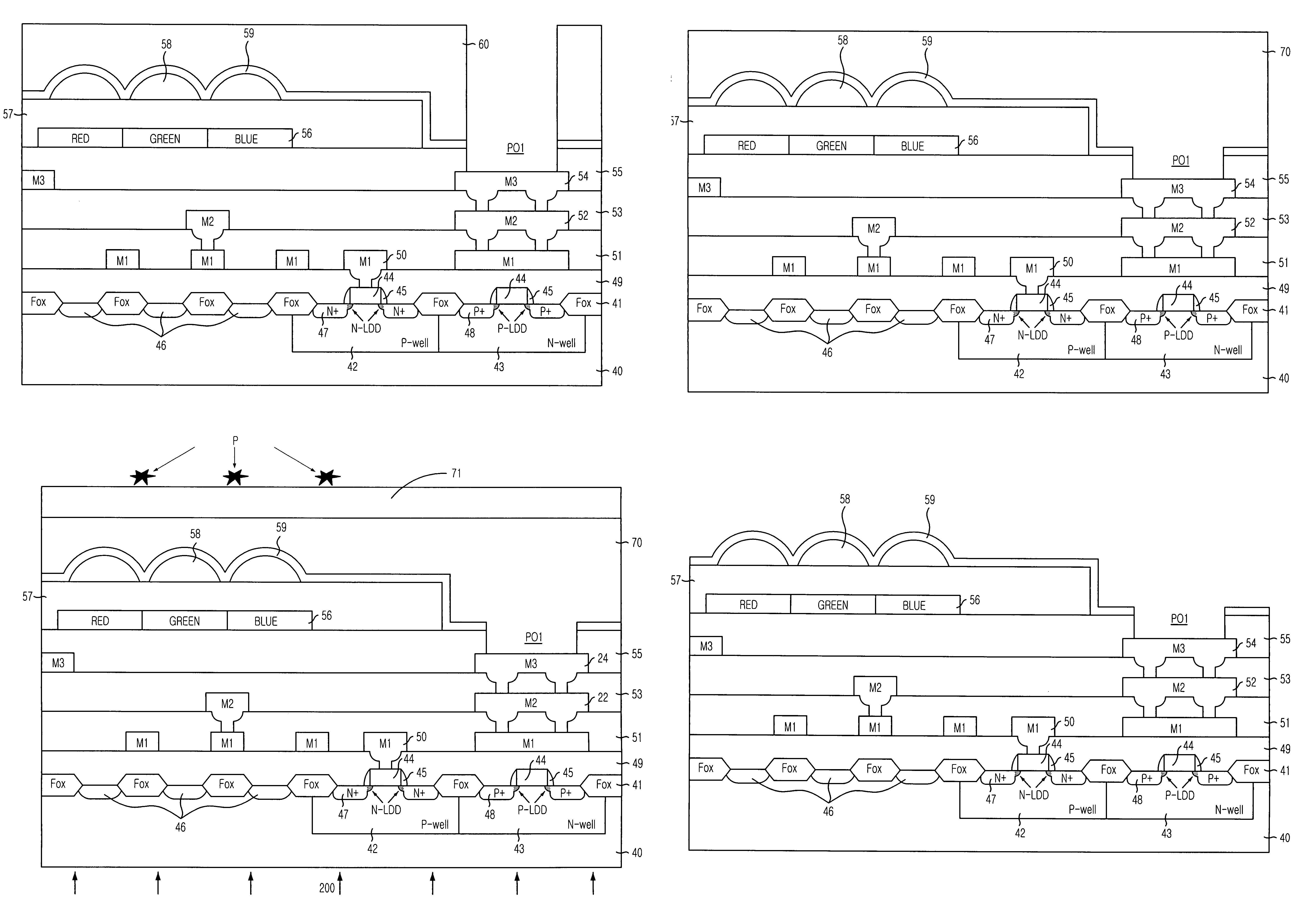
[0033]FIGS. 4A to 4D are cross-sectional views illustrating a method for fabricating an image sensor in accordance with an embodiment of the present invention.

[0034]Referring to FIG. 4A, field oxide layers 41 defining a filed region and an active region are formed over a substrate 40. A P-type well 42 and an N-type well 43 are formed using an ion implantation mask. Gate electrodes 44 and gate spacers 45 are formed over predetermined regions of the substrate 40. Unit pixels 46 including photodiodes are formed in a light sensing region, N-type ion implantation regions 47 and P-type ion implantation regions 48 with lightly doped drain (LDD) regions are formed. The N-type ion implantation regions 47 and P-type ion implantation regions 48 correspond to source / drain regions of transistors.

[0035]An inter-layer insulation layer 49 is formed over the above...


PUM


Abstract

Provided is a method for fabricating an image sensor using a wafer back grinding process. The method includes: forming a microlens protection layer over a substrate structure including a light sensing device and other associated devices; opening a pad open unit of the substrate structure using a mask; removing the mask; forming a photoresist layer over the substrate structure with the microlens protection layer; gluing a tape on the photoresist layer; performing a wafer back grinding process; and removing the tape and the photoresist layer.

Description

[0001]This application relies for priority upon U.S. Provisional Patent Application No. 60 / 669,198 filed on Apr. 6, 2005, the contents of which are herein incorporated by reference in its entirety.FIELD OF THE INVENTION[0002]The present invention relates to a method for fabricating an image sensor; and more particularly, to a method for fabricating an image sensor using a wafer back grinding process.DESCRIPTION OF RELATED ARTS[0003]Generally, image sensors convert an optical image into an electric signal. There are two types of an image sensor: a charge coupled device and complementary metal oxide semiconductor (CMOS) image sensor. In charge coupled devices (CCD), charge carriers are stored into or transferred from metal oxide semiconductor (MOS) capacitors closely disposed to each other. In CMOS image sensors (CIS), using CMOS technology including a control circuit and a signal processing circuit as a peripheral circuit, MOS transistors are prepared as many as the number of pixels,...

Claims


Application Information

Patent Timeline
Patent Type & Authority Patents(United States)
IPC IPC(8): H01L21/00
CPCH01L27/14685H01L27/14627
Inventor KIM, EUN-JIKWON, KYOUNG-KUK
Owner INTELLECTUAL VENTURES II
Why Eureka
Try Eureka