Electrostatic discharge protection circuit and semiconductor structure for electrostatic discharge

a protection circuit and electrostatic discharge technology, applied in the direction of overvoltage protection resistors, emergency protective arrangements for limiting excess voltage/current, etc., can solve the problem of insufficient turn-on efficiency, burn up or puncture circuit devices in an instant, and the effect of effectively bypassing esd current and excellent turn-on efficiency

Active Publication Date: 2008-11-11
UNITED MICROELECTRONICS CORP
View PDF7 Cites 6 Cited by
  • Summary
  • Abstract
  • Description
  • Claims
  • Application Information

AI Technical Summary

Benefits of technology

[0010]Accordingly, the present invention is directed to an electrostatic discharge (ESD) protection circuit, wherein the bypass circuit thereof comprises a diode to keep the voltage of the substrate terminal of the transistor stable so as to constantly turning on the transistor for bypassing the current. The ESD protection circuit of the present invention has an excellent turn-on efficiency, and can effectively bypass the ESD current.
[0011]In addition, the present invention is directed to a semiconductor structure related to ESD protection. The semiconductor structure comprises a diode for keeping the voltage of the substrate terminal of the transistor stable so as to constantly turning on the transistor for bypassing the current. The ESD protection circuit of the present invention has good turn-on efficiency, and can effectively bypass the ESD current.

Problems solved by technology

As a result, the minimized integrated circuits are more vulnerable to electrostatic discharge (ESD).
When ESD is received by circuit devices, a huge voltage or current flows through the circuit devices in a very short time, thereby may burn up or puncture the circuit devices in an instant.
As a result, its turn-on efficiency is not rapid enough, therefore causing puncturing or burning of the ESD protection circuit.
Also, the ESD protection circuit may not protect the internal devices of the integrated circuit.
Though the disadvantage in the circuit of FIG. 1A is improved, the bypassed ESD current is not sufficient while a small ESD voltage is received.

Method used


Image

  • Electrostatic discharge protection circuit and semiconductor structure for electrostatic discharge
  • Electrostatic discharge protection circuit and semiconductor structure for electrostatic discharge
  • Electrostatic discharge protection circuit and semiconductor structure for electrostatic discharge

Examples


Embodiment Construction

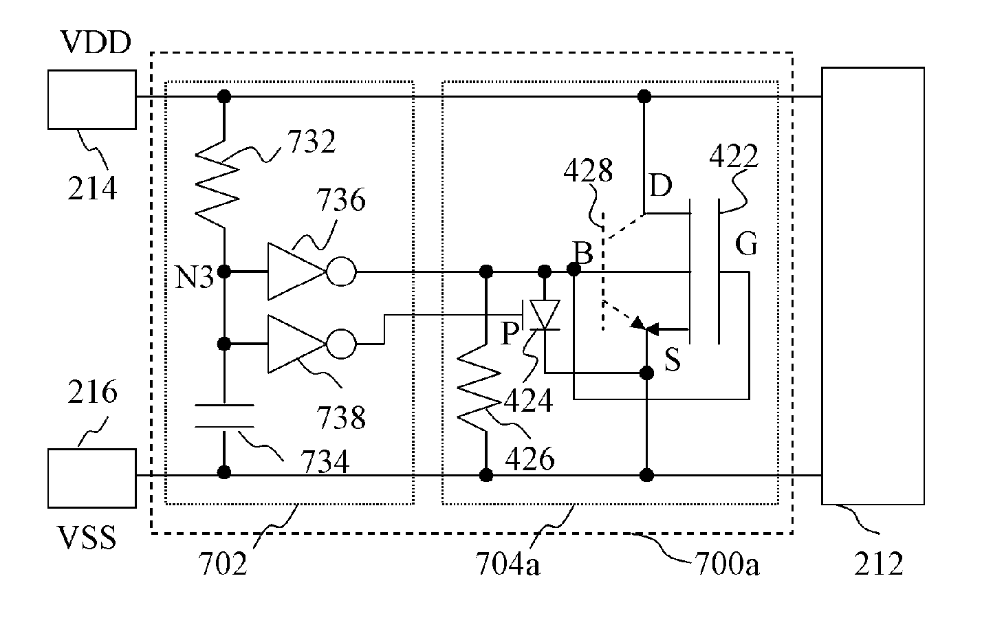
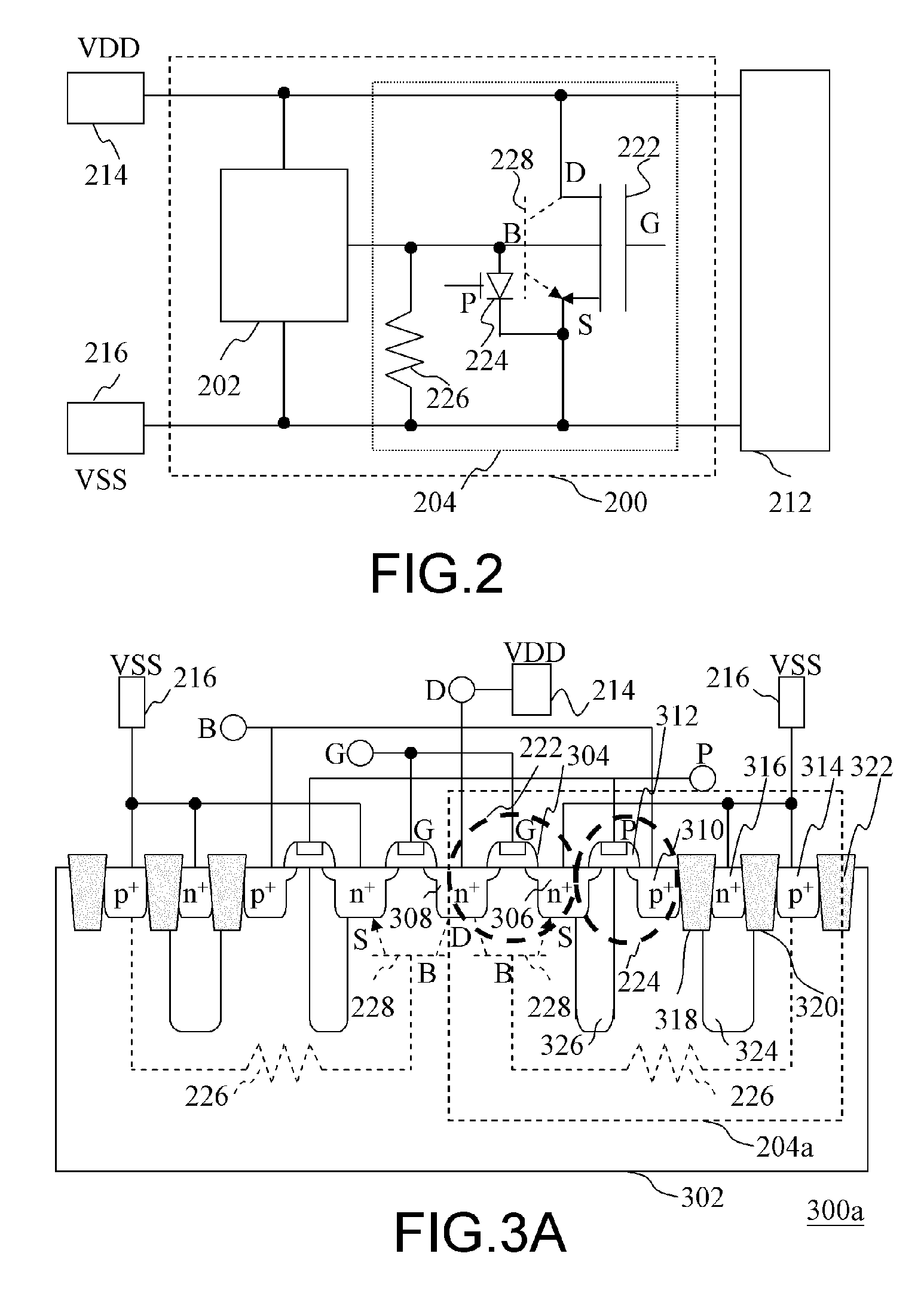
[0042]FIG. 2 is a schematic drawing showing an electrostatic discharge (ESD) protection circuit according to an embodiment of the present invention. Referring to FIG. 2, the ESD protection circuit 200 of the present invention comprises a detection circuit 202 and a bypass circuit 204, for example. The detection circuit 202 is coupled to the pads 214 and 216 of the integrated circuit 212 to detect whether there is an ESD current between the pads 214 and 216 or not. The bypass circuit 204 is coupled between the pads 214 and 216, and to the output terminal of the detection circuit 202 so as to bypass the ESD current. In an embodiment of the present invention, the pad 214 is coupled to the voltage VDD, and the pad 216 is coupled to the voltage VSS. Note that the integrated circuit 202, and the pads 214 and 216 are only embodiments of the present invention. The present invention, however, is not limited thereto. The present invention is applicable to any apparatus which requires an ESD p...


PUM


Abstract

An electrostatic discharge (ESD) protection circuit including a detection circuit for detecting an ESD current and a bypass circuit for bypassing the ESD current is provided. The detection circuit and the bypass circuit are coupled between a first pad and a second pad. The bypass circuit comprises a transistor, a diode, and a resistor. The drain of the transistor is coupled to the first pad. The source of the transistor is coupled to the second pad and a cathode of the diode. The substrate terminal of the transistor is coupled to an anode of the diode and an output terminal of the detection circuit. The resistor is coupled between the substrate terminal and the second pad. The diode keeps the voltage of the substrate terminal sufficient for turning on the transistor.

Description

BACKGROUND OF THE INVENTION[0001]1. Field of the Invention[0002]The present invention relates to an electrostatic discharge (ESD) protection circuit, and more particularly to an ESD protection circuit, an ESD protection apparatus, and a semiconductor structure adapted for ESD protection.[0003]2. Description of the Related Art[0004]Lately, with the advance of semiconductor technology, the integration of semiconductor devices has been increased by shrinking the line width and increasing the number of deposited film layers. However, while dimensions of integrated circuits shrink, the tolerable currents for circuits are also reduced. As a result, the minimized integrated circuits are more vulnerable to electrostatic discharge (ESD). When ESD is received by circuit devices, a huge voltage or current flows through the circuit devices in a very short time, thereby may burn up or puncture the circuit devices in an instant.[0005]In order to avoid ESD damage, ingeneral an ESD protection circu...

Claims


Application Information

Patent Timeline
Patent Type & Authority Patents(United States)
IPC IPC(8): H02H9/00H02H1/00H02H1/04H02H3/08H02H3/22H02H7/12H02H9/02H02H9/06
CPCH01L27/0266
Inventor CHEN, SHIAO-SHIEN
Owner UNITED MICROELECTRONICS CORP
Why Eureka
Try Eureka