

Method of laser annealing using linear beam having quasi-trapezoidal energy profile for increased depth of focus
a laser annealing and quasi-trapezoidal energy technology, applied in the field of annealing, can solve the problems of inconvenience, long processing time, affecting the display performance of the liquid crystal display device,
- Summary
- Abstract
- Description
- Claims
- Application Information
AI Technical Summary
Benefits of technology
Problems solved by technology
Method used
Image

Examples
embodiment 1
[0116]In this embodiment, a silicon film is used as a semiconductor material. A description will be made of a technique of improving the crystallinity of a silicon film by illuminating it with laser light.
[0117]First, an apparatus will be described.
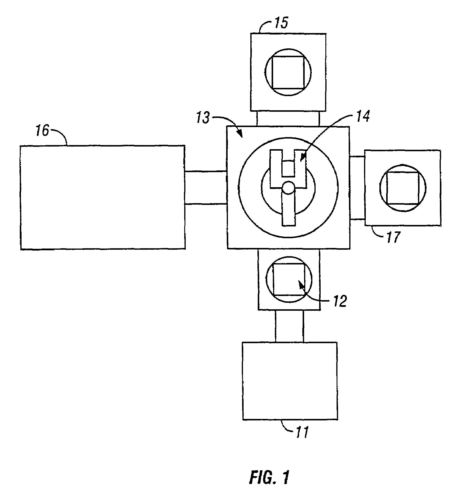
[0118]FIG. 1 shows the concept of a laser annealing apparatus used in this embodiment, which is of a multi-chamber type. Each substrate is input through a loader / unloader chamber 11, and then properly positioned in an alignment chamber 12. The substrate is then sequentially transferred to respective chambers via a transfer chamber 13 by means of a substrate transfer robot 14 that is provided in the transfer chamber 13, and processed in the respective chambers.
[0119]That is, a substrate is first input to a heat treatment chamber 15. After being subjected to a heat treatment, the substrate is subjected to laser annealing in a laser annealing chamber 16, cooled in a slow cooling chamber 17, and then moved to the loader / unloader chamber 11.
[0...
embodiment 2
[0161]This embodiment is directed to a case where a plurality of island-like patterned regions that are amorphous silicon films, on a glass substrate are converted by laser annealing into substantially single-crystalline silicon films, which are used as active layers of thin-film transistors.
[0162]As in the case of the first embodiment, the laser annealing apparatus of FIG. 1 is used in this embodiment.
[0163]An oscillator of type 3000-308 produced by Lambda Physic Corp. is used, which emits XeCl excimer laser light (wavelength: 308 nm; pulse width 26 ns). Naturally, other excimer lasers and other types of laser can be used as long as they are of a pulsed oscillation type.
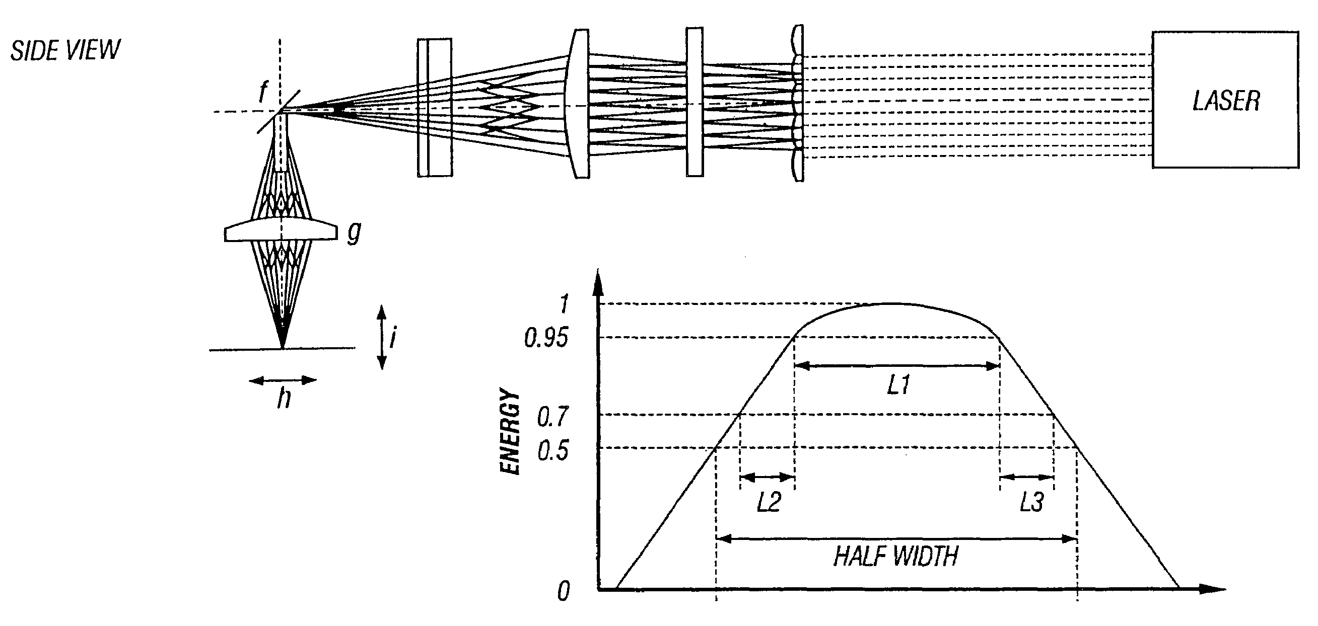
[0164]To transform the shape of an emitted laser beam, it is input to an optical system as shown in FIG. 3.
[0165]A laser beam, which assumes a rectangle of about 3×2 cm2 immediately before entering the optical system, is shaped into a long and narrow beam (i.e., linear beam) of 10 to 30 cm in length and 0.01 to 0.3 ...
embodiment 3
[0214]This embodiment uses the laser annealing apparatus of FIG. 1.
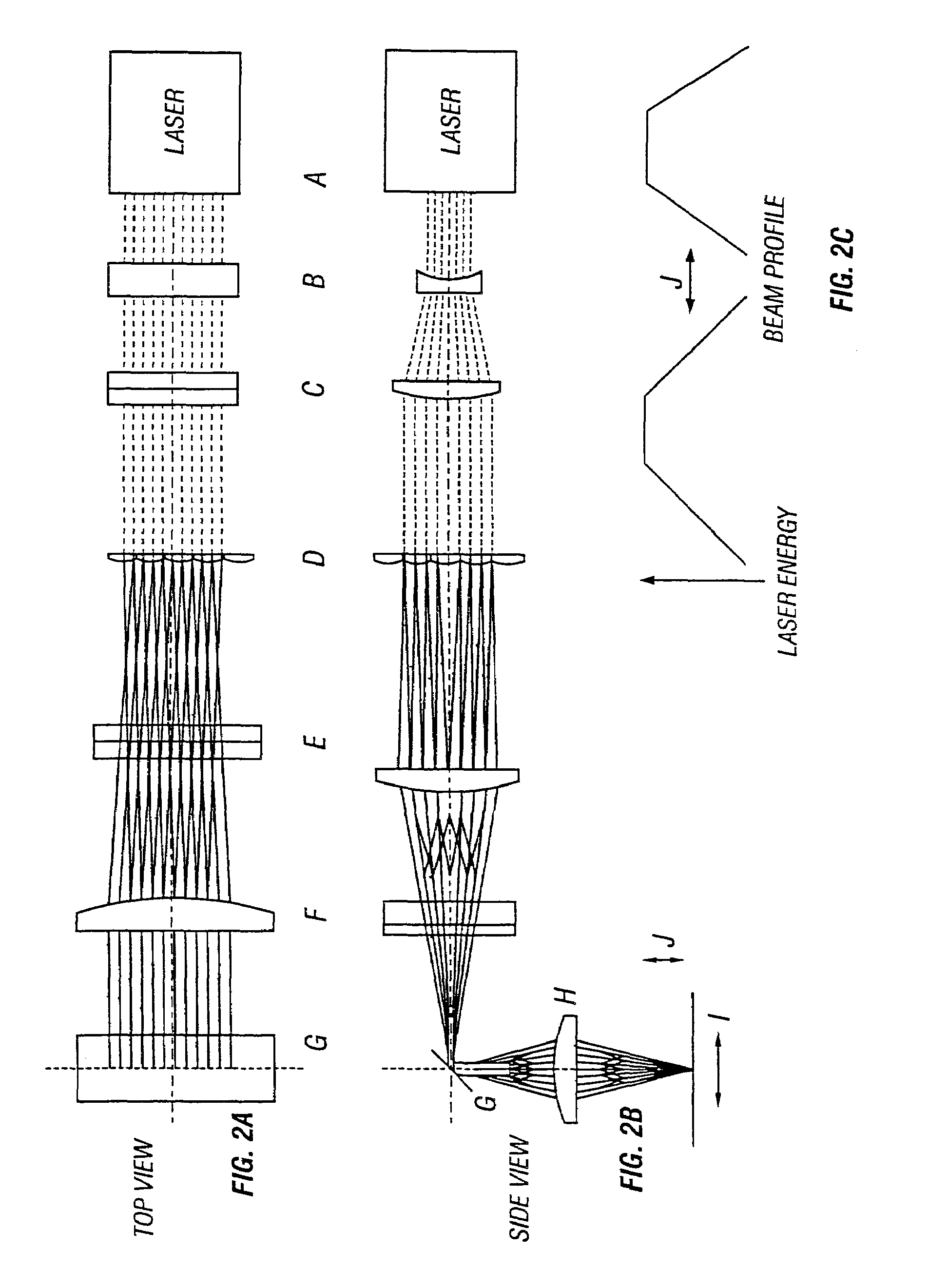
[0215]FIG. 9 shows an example of an optical system for laser annealing used in this embodiment.
[0216]The optical system of FIG. 9 is composed of the following components. An excimer laser beam generating means K (pulse laser beam generating means) generates an excimer laser beam. Beam expanders L and M expand the excimer laser beam. A compound-eye-like fly-eye lens N expands the laser beam in a sectional manner. A first cylindrical lens O converges the laser beam into a line shape. A second cylindrical lens P improves the uniformity of the linear laser beam in its longitudinal direction. A stage S is moved in direction T indicated by an arrow in FIG. 9 in a state that a substrate bearing an illumination object on its surface is placed thereon.
[0217]In FIG. 9, a path-folding mirror Q and a cylindrical lens R allow laser processing to be performed on the object placed on the stage S.
[0218]In this embodiment, the interv...
PUM
 Abstract
Description
Claims
Application Information