Test structures and method of defect detection using voltage contrast inspection

a voltage contrast inspection and test structure technology, applied in the field of semiconductor fabrication, can solve the problems of nfet and pfet structures not being similar devices of n-type field effect transistors (nfets) not working, and nfet and pfet structures cannot be inspected in the same scan, so as to achieve short learning cycles

Inactive Publication Date: 2008-11-25
INT BUSINESS MASCH CORP
View PDF14 Cites 95 Cited by
  • Summary
  • Abstract
  • Description
  • Claims
  • Application Information

AI Technical Summary

Benefits of technology

[0011]Test structures and a method for voltage contrast (VC) inspection are disclosed. In one embodiment, the test structure includes: a gate stack that is grounded by a ground to maintain the gate stack in an off state during VC inspection, which allows NFET defect detection using VC inspection prior to contact dielectric deposition. The test structure may alternatively include a gate stack that is biased by a bias to maintain the gate stack in an on state during VC inspection. The method may detect source-to-drain shorts in a transistor using VC inspection by providing a gate stack over a source and drain region of the transistor, in which the gate and source electrodes are grounded by a ground to maintain a channel under the gate stack in an off state during VC inspection; and inspecting the transistor using voltage contrast inspection. If the drain of the NFET brightens during VC inspection, this indicates a source to drain short. This inspection allows much shorter learning cycles for source to drain shorts.

Problems solved by technology

Transistor level defects such as dislocations and silicide pipes causing source to drain shorts is a problem in state of the art microelectronic fabrication due to the small scale of today's state of the art transistors.
Unfortunately, a similar device for an n-type field effect transistor (NFET) does not work because under electron extraction conditions (i.e., where a positive charge is induced on the surface), the gate of the device charges up just like any other exposed floating structure.
Another drawback of operating in electron retarding conditions is that the PFETs would now turn on.
Therefore, NFET and PFET structures could not be inspected in the same scan.
One drawback to this approach is that substantial additional processing is required causing a substantial time penalty in the learning cycle and substantial additional investigative work to identify the failure once detected.
This approach, however, requires substantially more time for additional processing, test and then failure analysis.

Method used


Image

  • Test structures and method of defect detection using voltage contrast inspection
  • Test structures and method of defect detection using voltage contrast inspection
  • Test structures and method of defect detection using voltage contrast inspection

Examples


Embodiment Construction

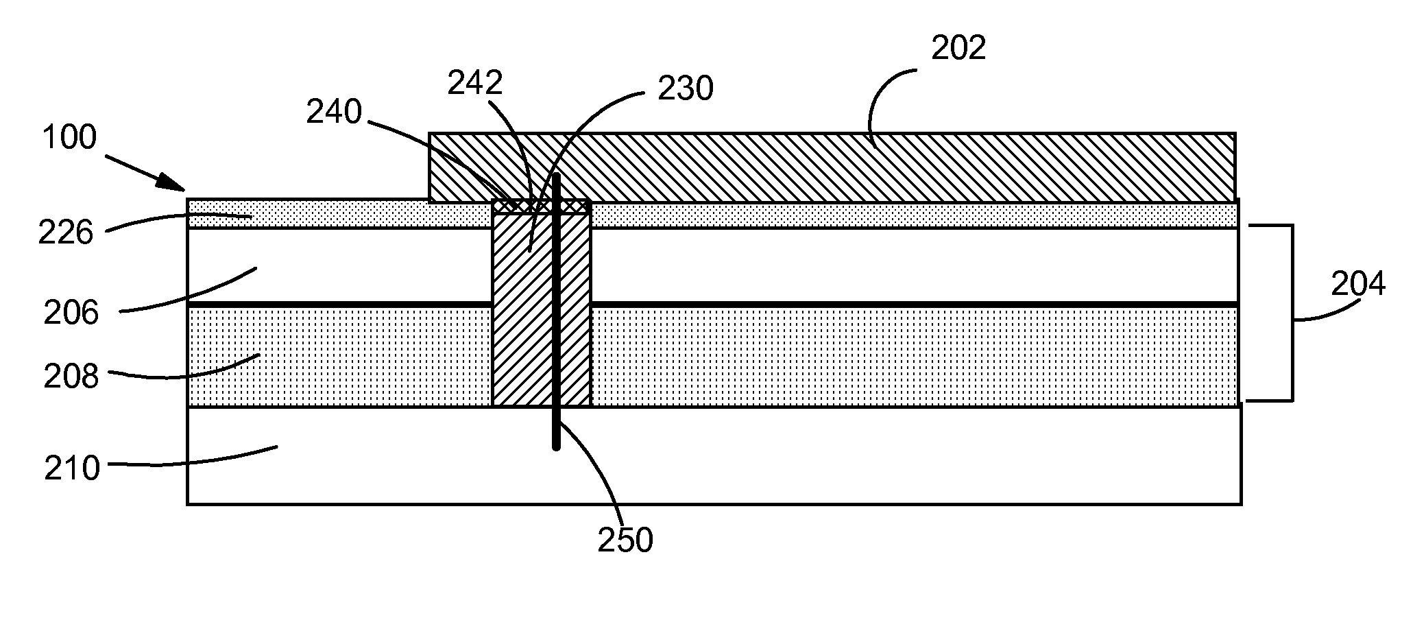
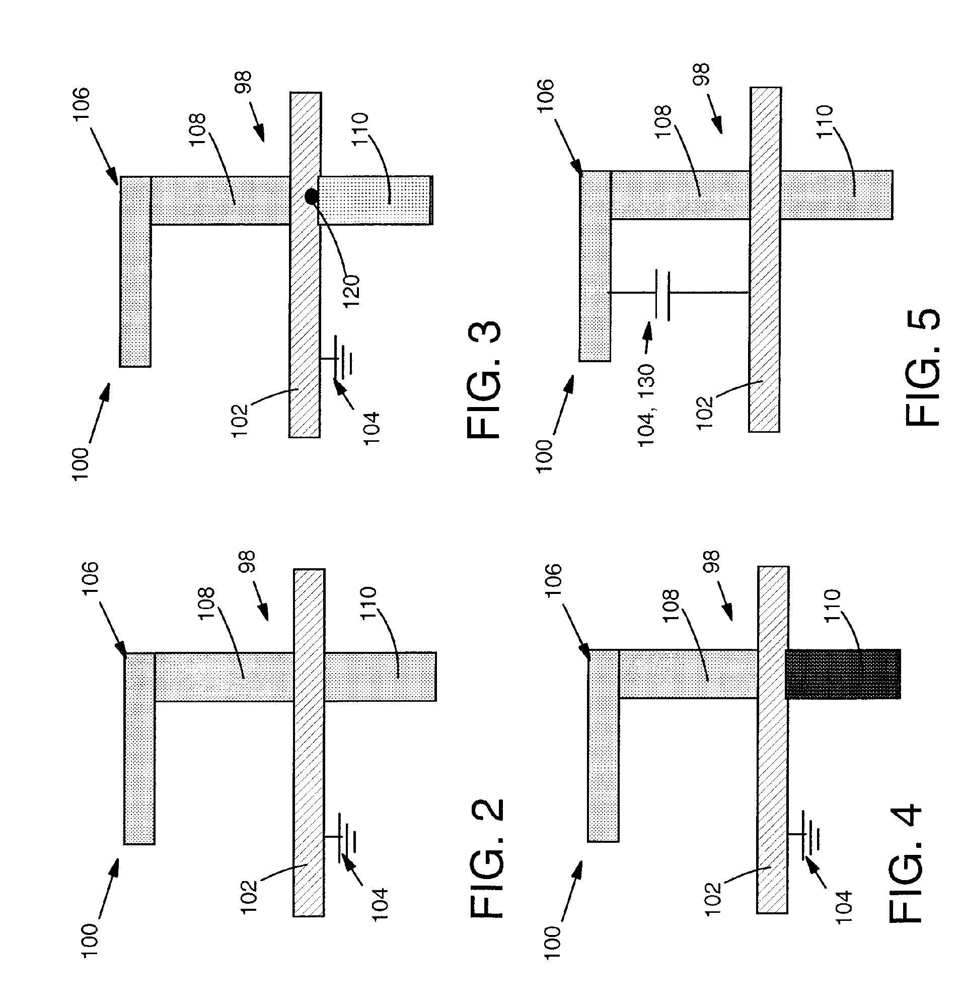
[0026]Turning to FIG. 2, as indicated above, embodiments of the invention provide test structures and a method for voltage contrast (VC) inspection of a transistor 98 (FIG. 2). In one embodiment, a test structure 100 includes: a gate stack 102, e.g., of polysilicon, that is grounded by a ground 104 to maintain a channel (not shown) under gate stack 102 in an off state during VC inspection. Test structure 100 may further include an active region 106 including a source region 108 and a drain region 110. Where ground 104 is part of an n-type field effect transistor (NFET) 98, it prevents a channel (not visible, where gate stack 102 and active region 106 intersect) of the NFET from conducting during VC inspection using electron extraction conditions if no defect exists in a gate dielectric and the channel of the NFET. In contrast, where gate stack 102 is part of a p-type field effect transistor (PFET) 98, it prevents a channel (not visible, where gate stack 102 and active region 106 int...


PUM


Abstract

Test structures and a method for voltage contrast (VC) inspection are disclosed. In one embodiment, the test structure includes: a gate stack that is grounded by a ground to maintain the gate stack in an off state during VC inspection, which allows NFET defect detection using VC inspection prior to contact dielectric deposition. The test structure may alternatively include a gate stack that is biased by a bias to maintain the gate stack in an on state during VC inspection. The method may detect source-to-drain shorts in a transistor using VC inspection by providing a gate stack over a source and drain region of the transistor that is grounded by a ground to maintain the gate stack in an off state during VC inspection; and inspecting the transistor using voltage contrast. If the drain of the NFET brightens during VC inspection, this indicates a source to drain short.

Description

[0001]This application relates to U.S. patent application Ser. No. 11 / 308,408, filed Mar. 22, 2006, entitled GROUNDING FRONT-END-OF-LINE STRUCTURES ON A SOI SUBSTRATE, which is hereby incorporated herein by reference.BACKGROUND OF THE INVENTION[0002]1. Technical Field[0003]The invention relates generally to semiconductor fabrication, and more particularly, to test structures and a method of detecting defects using voltage contrast inspection.[0004]2. Background Art[0005]In-line voltage contrast (VC) inspection is a powerful technique for detecting and isolating yield limiting defects in the semiconductor fabricating industry. In-line VC inspection includes scanning the wafer surface in which test structures exist with a scanning electron microscope (SEM). As the inspection proceeds, the SEM induces charge on all electrically floating elements whereas any grounded elements remain at zero potential. This potential difference is visible to the SEM. In particular, for electron landing e...

Claims


Application Information

Patent Timeline
Patent Type & Authority Patents(United States)
IPC IPC(8): G01R31/02G01R31/26H01L23/62
CPCG01R31/2884G01R31/307
Inventor PATTERSON, OLIVER D.ZHU, HUILONG
Owner INT BUSINESS MASCH CORP
Why Eureka
Try Eureka