Wafer grinding method

a technology of a wafer and a grinding method, which is applied in the direction of grinding machines, edge grinding machines, manufacturing tools, etc., can solve the problems of reducing productivity, increasing cost, and affecting yield, so as to improve yield, reduce productivity, and increase cost

Active Publication Date: 2008-12-09
DISCO CORP
View PDF5 Cites 19 Cited by
  • Summary
  • Abstract
  • Description
  • Claims
  • Application Information

AI Technical Summary

Benefits of technology

[0007]Accordingly, it is an object of the present invention to provide a wafer grinding method by which a processing for minimizing the generation of chipping of the outer peripheral edge of a wafer can be performed before a grinding step and without using any step or device other than that for grinding, with the result that an enhanced yield can be contrived without causing a lowering in productivity or a rise in cost.
[0010]The chipping of the outer peripheral edge, which is the problem to be solved by the present invention, is liable to be generated at the time of rough grinding in the first grinding step. However, in the first grinding step based on the present invention, only the region, corresponding to the device formation region, of the back side of the wafer is ground to form the recess and, at the same time, the periphery of the device formation region is left unground (left in the original thickness) to thereby form the annular projected part. Thus, in the first grinding step, the outer peripheral edge is not ground, so that chipping of the outer peripheral edge is not generated; therefore, the region corresponding to the device formation region, which is a major part of the wafer, can be roughly ground without any trouble.
[0011]Next, in the second grinding step, the annular projected part is ground in a collapsing manner by the second grindstone(s), to remove the annular projected part, and further the whole area of the back side of the wafer is ground to finish the back side into a flat state. Since the grinding amount relevant to the annular projected part is small and the grinding resistance in this instance is small, the grinding of the annular projected part can be conducted even with the second grindstone(s) for finishing. Due to the grinding with the second grindstone(s) for finishing, chipping of the outer peripheral edge would not be generated easily and, even if the chipping is generated, the depth of chipping is much smaller than that which might be generated during rough grinding, so that the influence of the chipping to the device formation region can be restrained.
[0014]According to the method based on the present invention, since grinding is conducted in such a manner as to restrain the generation of chipping of the outer peripheral edge of the wafer in the grinding process, chipping of the outer peripheral edge can be restrained as securely as possible, without using any step or device other than that for grinding, such as a step or device for cutting. As a result, in the process of grinding the back side of a wafer, an enhanced yield can be contrived without causing a lowering in productivity or a rise in cost.

Problems solved by technology

Meanwhile, since the wafer with its back side to be ground is preliminarily subjected to chamfering of the outer peripheral edge, the outer peripheral edge becomes knife edge-like in sectional shape after the wafer is thinned to or below one half of the original thickness, and, therefore, the outer peripheral edge is liable to be chipped during grinding.
More specifically, the step of removing the outer peripheral edge of the wafer at a stage before grinding of the back side of the wafer is added, and a device for this purpose is needed, which leads to a lowering in productivity and a rise in cost.

Method used


Image

  • Wafer grinding method
  • Wafer grinding method
  • Wafer grinding method

Examples


Embodiment Construction

[0028]Now, one embodiment of the present invention will be described below referring to the drawings.[0029][1] Semiconductor Wafer

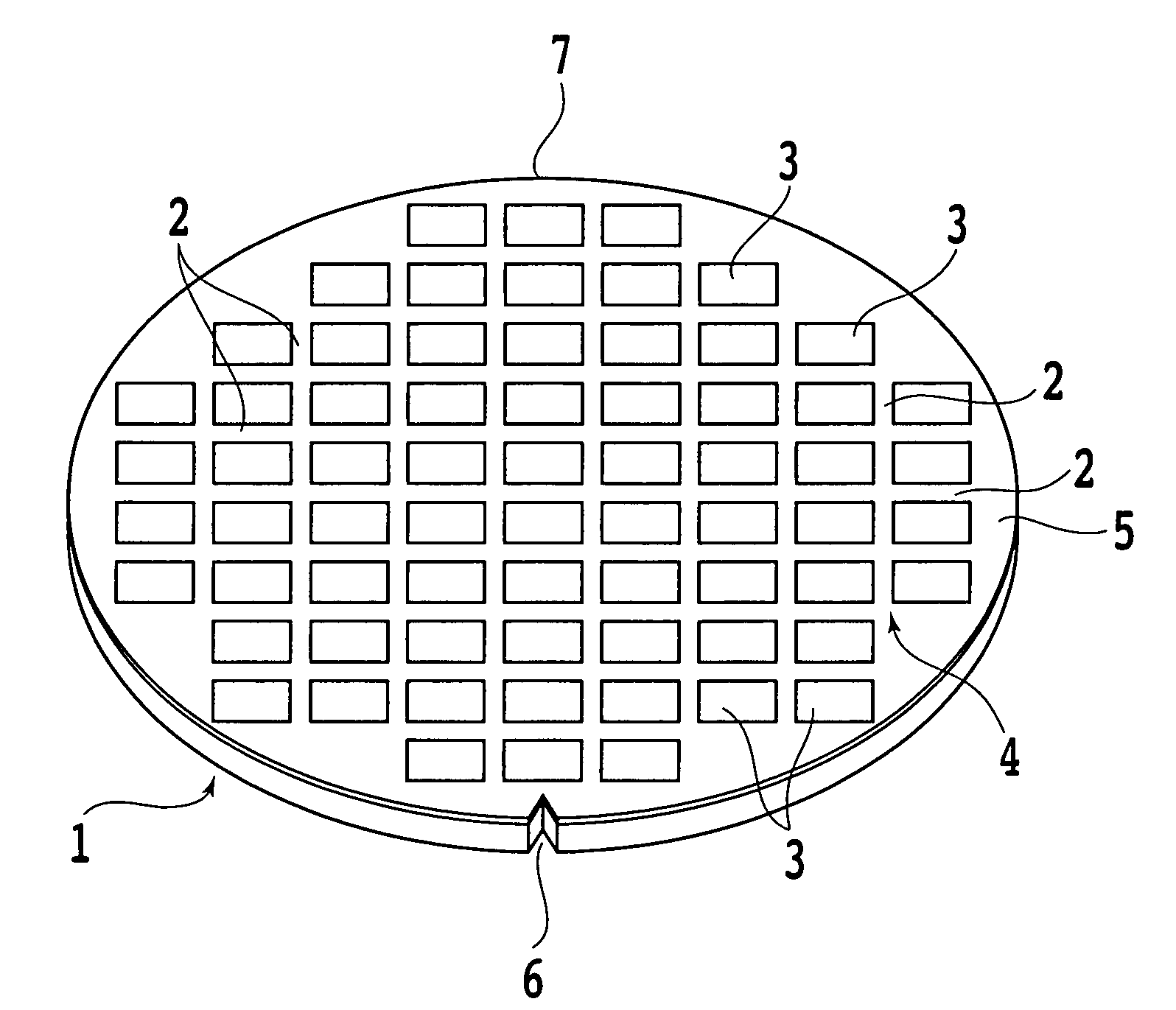
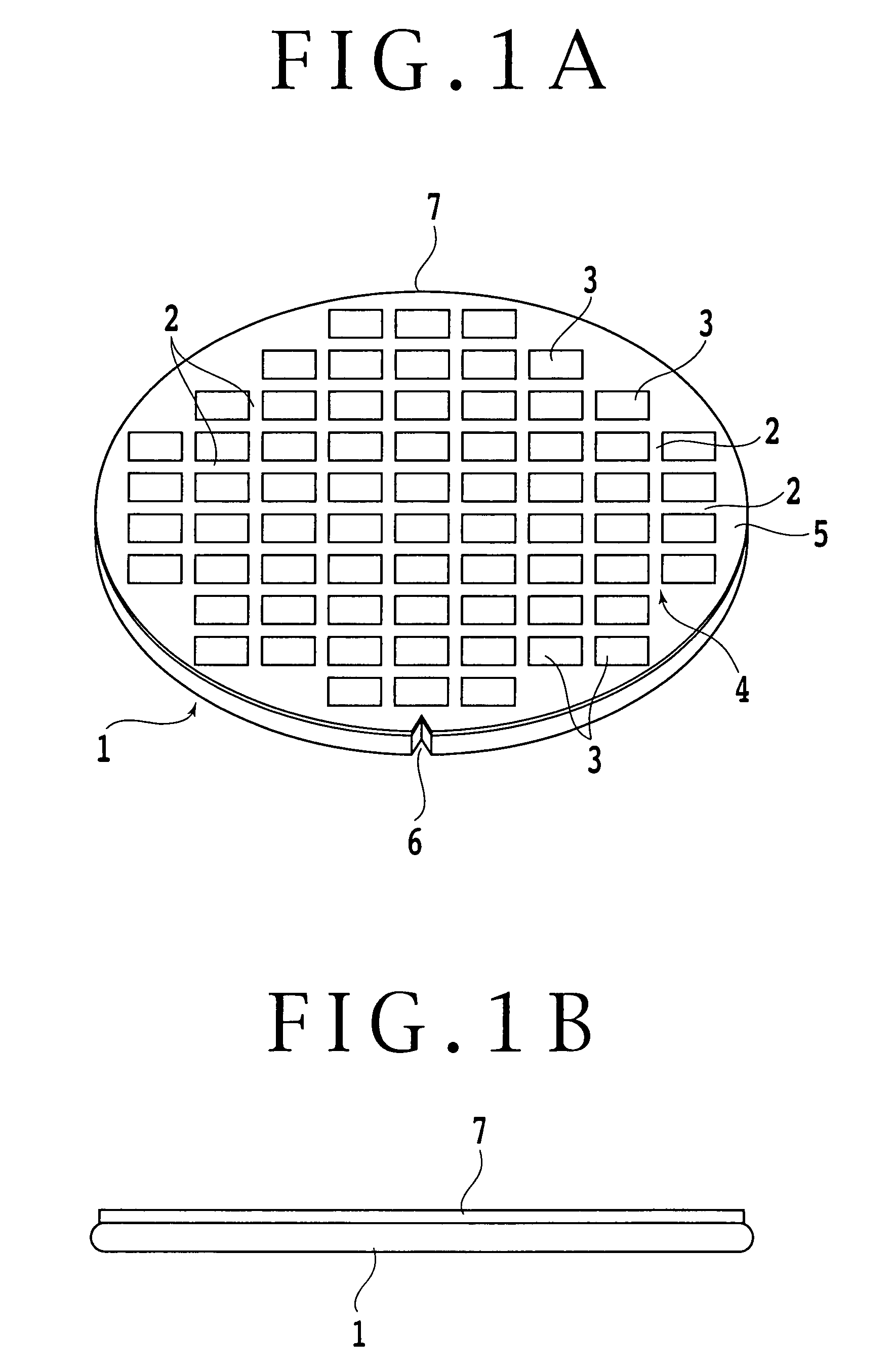
[0030]Symbol 1 in FIGS. 1A and 2B denotes a circular disk-like semiconductor wafer (hereinafter referred to simply as wafer) of which the whole area of the back side is to be ground by the wafer grinding method according to the one embodiment to be thinned to an objective thickness. The wafer 1 is a silicon wafer or the like, and its thickness before processing is about 600 to 700 μm, for example. On the face side of the wafer 1, a plurality of rectangular semiconductor chips (devices) 3 are demarcated by planned splitting lines 2 formed in a lattice pattern, and electronic circuits (not shown) such as ICs and LSIs are formed on the surfaces of the semiconductor chips 3. The outer peripheral edge of the wafer 4 is chamfered into a semicircular arc sectional shape so as to eliminate corners and to lower the possibility of damage thereto.

[0031]The plurality...


PUM

PropertyMeasurementUnit
thicknessaaaaaaaaaa
thicknessaaaaaaaaaa
thicknessaaaaaaaaaa

Abstract

A wafer grinding method is disclosed, in which only a region, corresponding to a device formation region, of the back side of a wafer is ground in rough grinding conducted first, while the part surrounding the region thus ground is left unground as an annular projected part, to prevent the outer peripheral edge of the wafer from becoming knife edge-like in shape. In the subsequent finish grinding, the annular projected part is ground and, further, the whole area of the back side of the wafer is ground to be flat. Chippings of the outer peripheral edge may be generated only during the finish grinding, whereby the chippings are prevented from occurring or limited to minute ones.

Description

BACKGROUND OF THE INVENTION[0001]1. Field of the Invention[0002]The present invention relates to a grinding method for grinding the back side of a wafer such as a semiconductor wafer to thin the wafer to a predetermined thickness, and particularly to an improving technology for minimizing the chipping of the outer peripheral edge of a wafer generated when the back side of the wafer is ground.[0003]2. Description of the Related Art[0004]In general, semiconductor chips of devices used for various electronic apparatus are each produced by a method in which rectangular regions are demarcated on the face side of a circular disk-like semiconductor wafer in a lattice pattern by planned splitting lines, electronic circuits such as ICs and LSIs are formed on the face side of these regions, then the back side of the wafer is ground to thin the wafer, and the wafer is cut and split (diced) along the planned splitting lines.[0005]Meanwhile, since the wafer with its back side to be ground is pre...

Claims


Application Information

Patent Timeline
Patent Type & Authority Patents(United States)
IPC IPC(8): B24B1/00
CPCB24B1/00B24B7/228
Inventor YOSHIDA, SHINJINAGAI, OSAMU
Owner DISCO CORP
Why Eureka
Try Eureka