Wafer grinding method
- Summary
- Abstract
- Description
- Claims
- Application Information
AI Technical Summary
Benefits of technology
Problems solved by technology
Method used
Image
Examples
Embodiment Construction
[0028] Now, one embodiment of the present invention will be described below referring to the drawings.
[1] Semiconductor Wafer
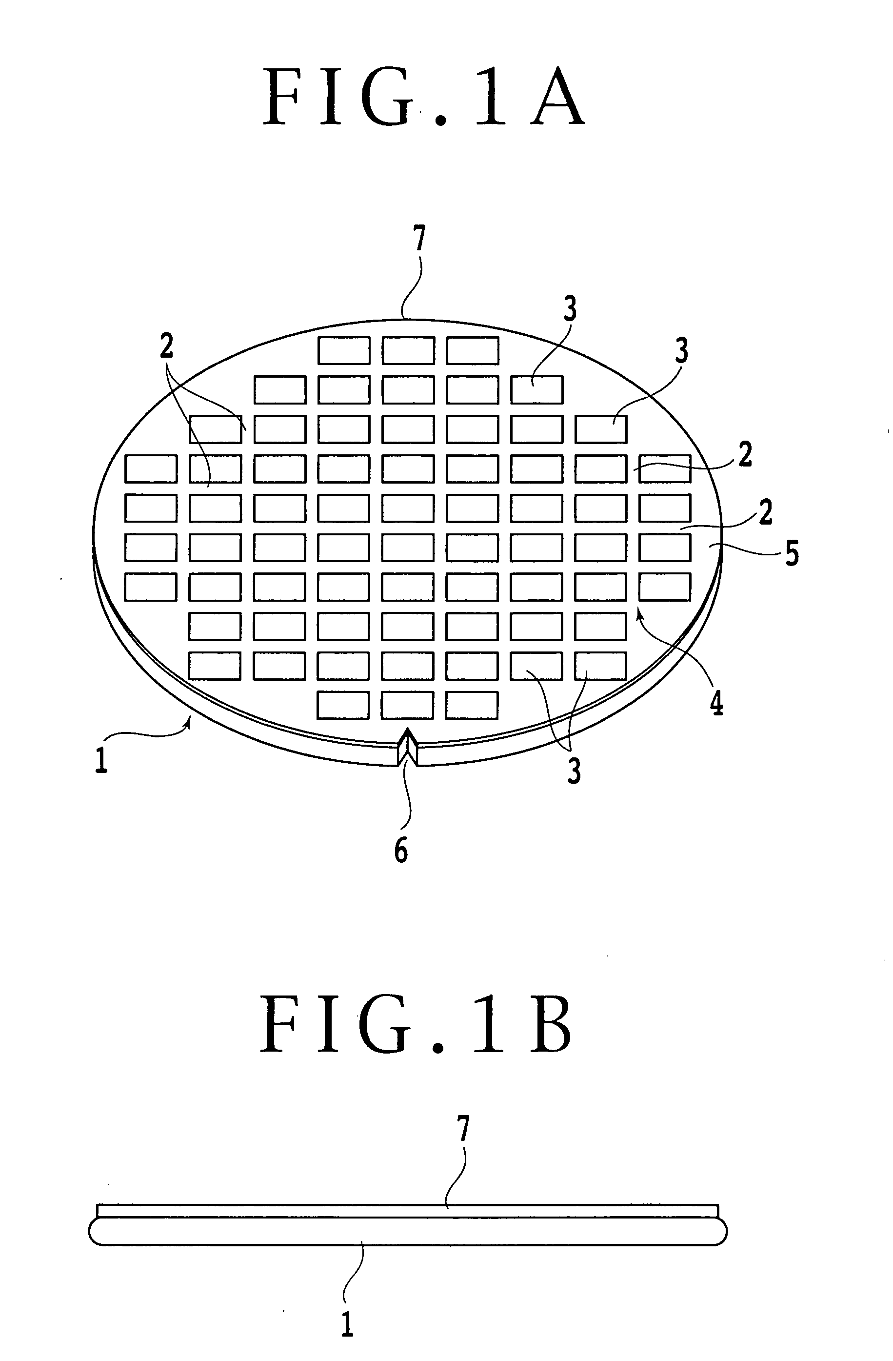
[0029] Symbol 1 in FIGS. 1A and 2B denotes a circular disk-like semiconductor wafer (hereinafter referred to simply as wafer) of which the whole area of the back side is to be ground by the wafer grinding method according to the one embodiment to be thinned to an objective thickness. The wafer 1 is a silicon wafer or the like, and its thickness before processing is about 600 to 700 μm, for example. On the face side of the wafer 1, a plurality of rectangular semiconductor chips (devices) 3 are demarcated by planned splitting lines 2 formed in a lattice pattern, and electronic circuits (not shown) such as ICs and LSIs are formed on the surfaces of the semiconductor chips 3. The outer peripheral edge of the wafer 4 is chamfered into a semicircular arc sectional shape so as to eliminate corners and to lower the possibility of damage thereto.
[0030] The pluralit...
PUM
| Property | Measurement | Unit |
|---|---|---|
| Diameter | aaaaa | aaaaa |
| Shape | aaaaa | aaaaa |
| Abrasive | aaaaa | aaaaa |
Abstract
Description
Claims
Application Information


