Field effect transistor

a field effect transistor and transistor technology, applied in transistors, semiconductor devices, electrical apparatus, etc., can solve the problems of floating body effects, space requirements in the arrangement of adjacent transistors, and restrictions in the design of integrated circuit arrangements, etc., to achieve convenient arrangement and good electrical properties

Active Publication Date: 2008-12-09
INFINEON TECH AG
View PDF8 Cites 0 Cited by
  • Summary
  • Abstract
  • Description
  • Claims
  • Application Information

AI Technical Summary

Benefits of technology

[0012]This invention provides a field effect transistor including a control region. The control region may be fabricated from monocrystalline material. Accordingly, the control region can be readily arranged in a monocrystalline semiconductor substrate. Moreover, it is possible for a control region of monocrystalline material to grow a monocrystalline dielectric epitaxially. In addition, a monocrystalline channel region can also be grown epitaxially on the dielectric. A “monocrystalline” field effect transistor can provide very good electrical properties. In one embodiment, the monocrystalline control region can be arranged in a monocrystalline substrate, which may contain multiple electrical semiconductor components.
[0016]In yet another embodiment of a field effect transistor, the channel region also comprises monocrystalline material. The channel region can thus be grown epitaxially on a monocrystalline dielectric. The channel region can be doped, however, the channel region may also be undoped, particularly in the case of dimensions in the nanometers range. In one refinement, the channel region has an extent of less than 20 nm transversely with respect to the control region. This measure gives rise to a fully depleted field effect transistor in which short-channel effects do not occur or occur only to a greatly reduced degree. The electrical properties of the field effect transistor are, therefore, particularly good.
[0020]In yet another embodiment, the memory cell does not contain an insulation collar, so that the production steps associated therewith can be obviated. However, as an alternative, an insulation collar may be formed to prevent parasitic transistors from arising if no other measures are taken.
[0022]The invention additionally relates to a method for producing a field effect transistor or for producing a memory cell. The above mentioned technical effects thus also hold true for the method. The method is particularly simple when firstly the transistor dielectric is grown epitaxially on a monocrystalline region for the control region and then the channel region is grown epitaxially on the transistor dielectric.

Problems solved by technology

This approach leads to restrictions in the design of the integrated circuit arrangement.
These disadvantages become even more evident in the case of field effect transistors for memory cells.
Problems from the customary approaches arise in regard to leakage associated with the connection regions buried in the trench (buried straps), the production steps for connection regions buried in the trench (buried straps), the space requirement in the arrangement of adjacent transistors, and floating body effects.
The channel region can be doped, however, the channel region may also be undoped, particularly in the case of dimensions in the nanometers range.

Method used


Image

  • Field effect transistor
  • Field effect transistor
  • Field effect transistor

Examples


Embodiment Construction

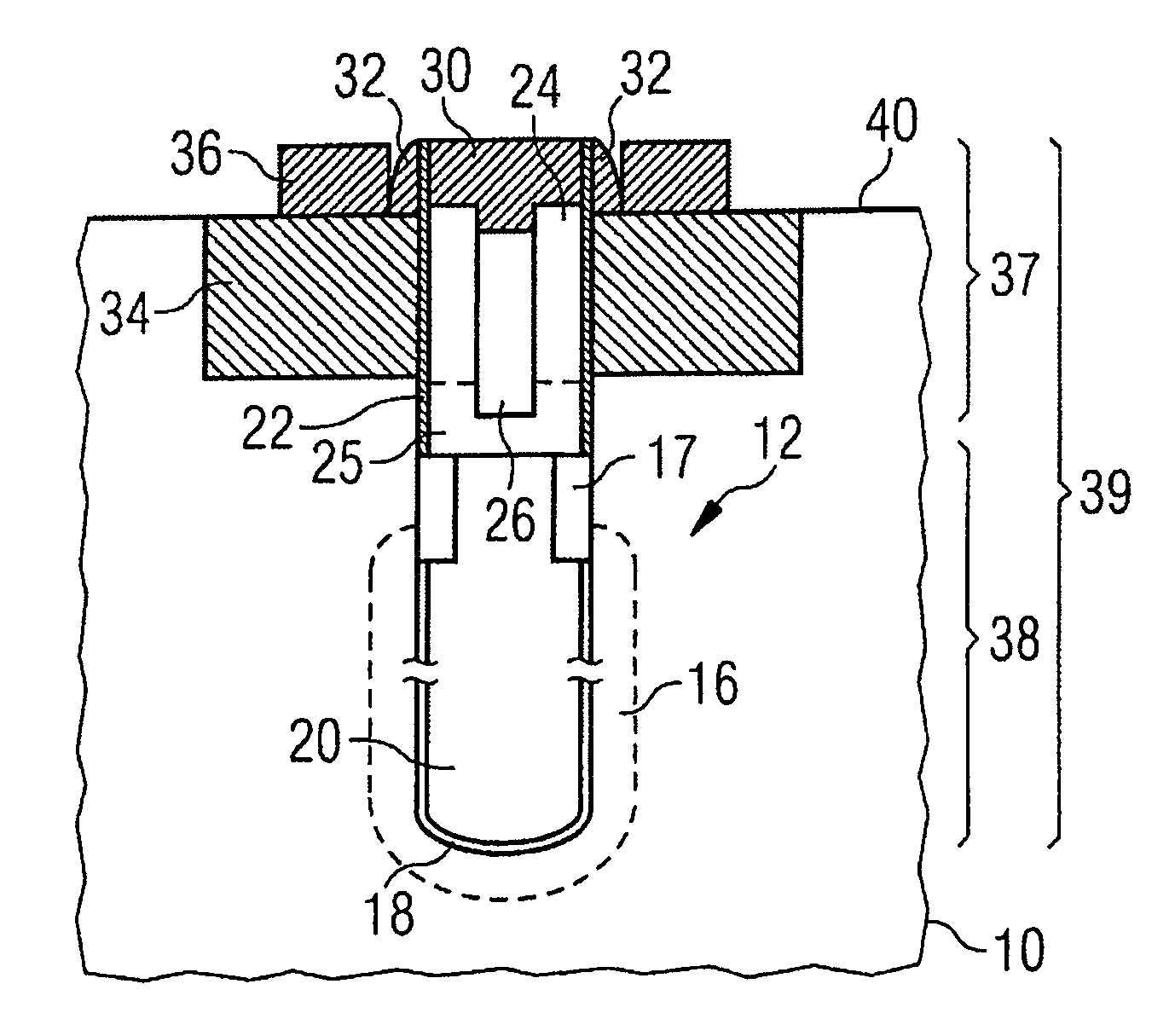
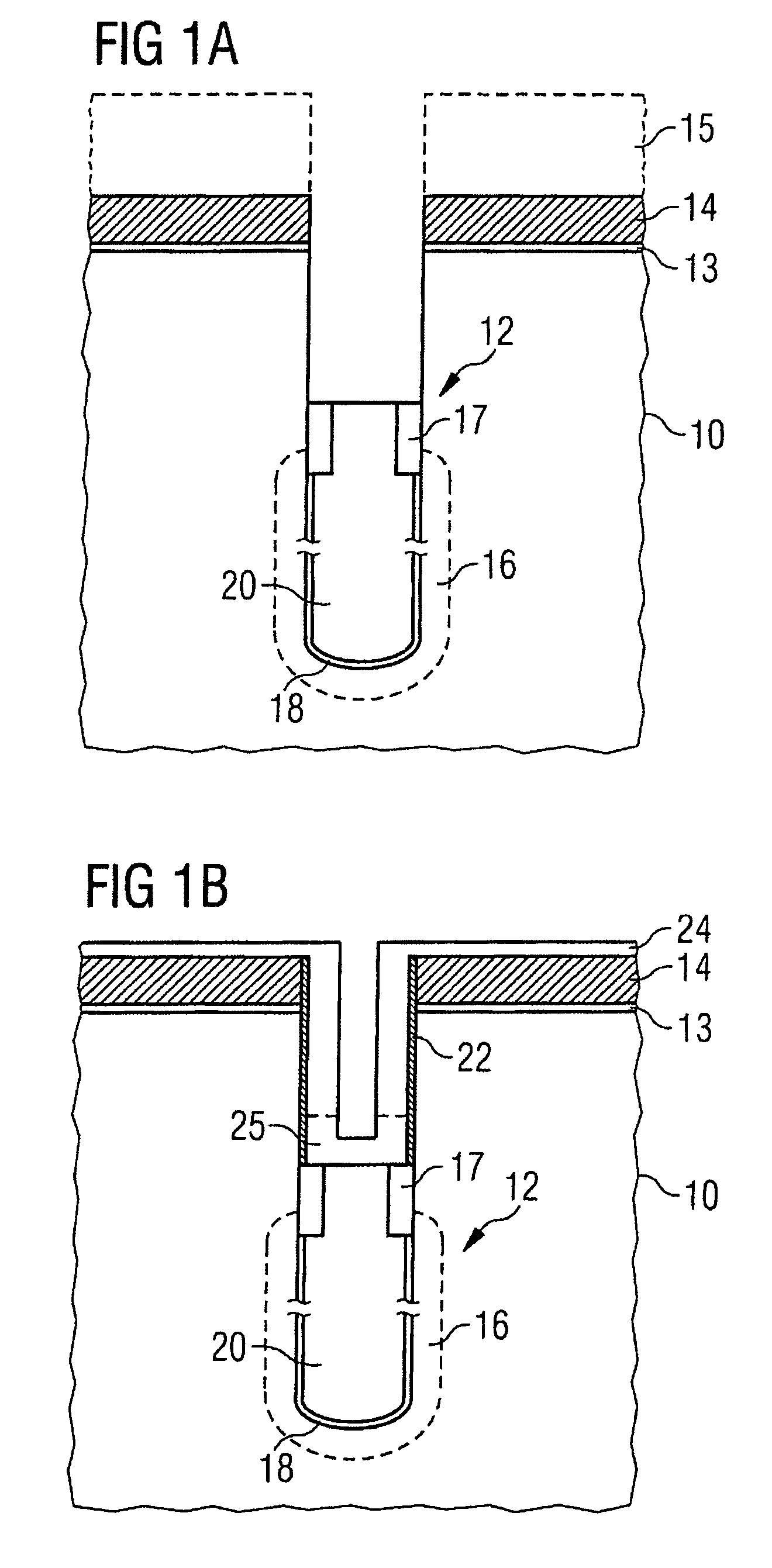
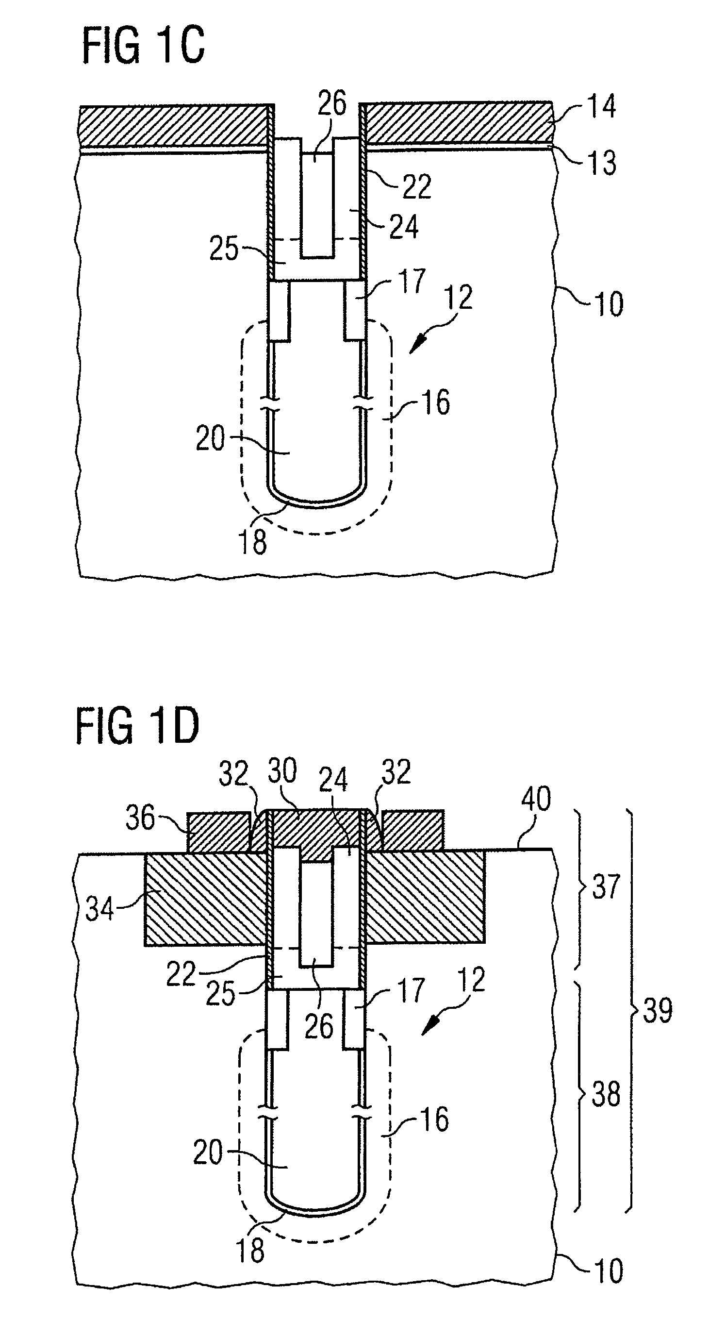
[0026]As illustrated in FIG. 1A, a silicon substrate 10 including a trench 12 is provided. A method for producing a multiplicity of deep trenches is performed in a known manner to provide the trench 12. The trench 12 has, for example, a depth lying between 6 μm and 10 μm. The diameter of the trench is, for example, less than 250 nm (nanometers). The trench 12 is illustrated in greatly shortened fashion in FIGS. 1A to 1D.

[0027]In order to produce the trench 12, a thin support layer 13, for example a silicon oxide layer having a thickness of 5 nm, is applied to the substrate 10. The thin support layer 13 has applied to it a thicker support layer 14, for example a silicon nitride layer having a thickness of 100 nm to 200 nm. A hard mask layer 15, for example made of TEOS (tetraethyl orthosilicate) is applied to the support layer 14. The hard mask layer 15 may have a thickness of greater than 500 nm. The hard mask layer 15, the thicker support layer 14, and the thin support layer 13 are...


PUM

PropertyMeasurementUnit
resistivityaaaaaaaaaa
depthaaaaaaaaaa
depthaaaaaaaaaa

Abstract

A field effect transistor is provided. The field effect transistor includes a channel region, electrically conductive channel connection regions, and a control region. The electrically conductive channel connection regions adjoin the channel region along with a transistor dielectric. The control region is separated from the channel region by the transistor dielectric. In addition, the control region may comprise a monocrystalline material.

Description

PRIORITY CLAIM[0001]This application is a continuation of international application PCT / EP2004 / 052216 filed Sep. 16, 2004, which claims priority to German Patent Application No. DE 10348006.4 Filed Oct. 15, 2003, both of which are incorporated in their entirety by reference herein.BACKGROUND[0002]1. Field of the Invention[0003]The invention relates to a field effect transistor.[0004]2. Description of Related Art[0005]A field effect transistor may commonly include a channel region, an electrically conductive region, and a control region. The electrically conductive regions adjoin the channel and the control region is separated from the channel region by a transistor dielectric that adjoins the channel region.[0006]The channel region is usually formed of a semiconductor material, for example a material whose resistivity lies between the resistivity of metals and the resistivity of insulators. Accordingly, the semiconductor material may have resistivity values of between approximately ...

Claims


Application Information

Patent Timeline
Patent Type & Authority Patents(United States)
IPC IPC(8): H01L27/108H01L21/8242
CPCH01L27/1082H01L27/10823H01L27/10832H01L27/10841H01L27/10858H01L27/10864H01L29/4916H01L29/66666H01L29/7827H01L27/10876Y10T29/41H01L29/161H01L29/517H01L29/518H10B12/33H10B12/373H10B12/34H10B12/395H10B12/036H10B12/0383H10B12/053
Inventor TEWS, HELMUT
Owner INFINEON TECH AG
Why Eureka
Try Eureka