Organic light-emitting device

a light-emitting device and organic compound technology, applied in the direction of discharge tube luminescnet screens, discharge tube/lamp details, electric discharge lamps, etc., can solve the problems of degradation of the hole-transporting layer, insufficient stability of the existing device, and the inability to apply the device to the light-emitting device for emitting green light or blue light, etc., to achieve wide band gap, reduce emission intensity, and high emission efficiency

Active Publication Date: 2008-12-16
CANON KK
View PDF3 Cites 7 Cited by
  • Summary
  • Abstract
  • Description
  • Claims
  • Application Information

AI Technical Summary

Benefits of technology

[0009]It is, therefore, an object of the present invention to alleviate the lowering in emission intensity due to continuous driving of an organic light-emitting device, in particular, an organic light-emitting device using a light-emitting layer material having a wide band gap, while maintaining a high emission efficiency.
[0018]According to the present invention, the lowering in emission intensity due to continuous driving can be alleviated even in an organic light-emitting device using a light-emitting layer material having a wide band gap while a high emission efficiency is maintained.

Problems solved by technology

However, particularly when considering its application to, for example, a full-color display, the stability of the existing device is not sufficient for putting into practical use, so that an additional improvement in stability has been needed.
However, according to this technique, the rubrene contained in the hole-transporting layer emits a strong yellow light, so that the device cannot be applied to a light-emitting device for emitting a green light or blue light.
One of the causes for the degradation of an organic light-emitting device by driving is that a hole-transporting material which constitutes a hole-transporting layer is degraded by going through a triplet excited state.
Moreover, the triplet excited state generally has a long lifetime of an order of ms or more, so that degradation such as decomposition due to going through a triplet excited state and the like becomes a problem.
However, in cases where a material having a large energy gap E1 is used as is the case where the emission color is blue, such energy relationship is sometimes not satisfied, so that the degradation of the hole-transporting material becomes significant.

Method used


Image

  • Organic light-emitting device
  • Organic light-emitting device
  • Organic light-emitting device

Examples


example 1

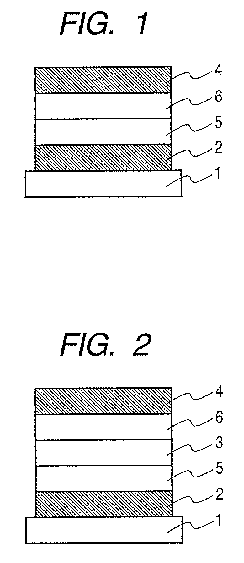
[0082]An organic light-emitting device with a configuration shown in FIG. 2 was produced.

[0083]A transparent conductive support substrate was prepared which had a film of indium tin oxide (ITO) with a thickness of 120 nm as an anode 2 formed on a glass sheet as a substrate 1 by a sputtering method. The transparent conductive support substrate was ultrasonically cleaned sequentially with acetone and isopropyl alcohol (IPA), subsequently cleaned with boiled IPA, was dried, was further cleaned with UV / ozone, and was used.

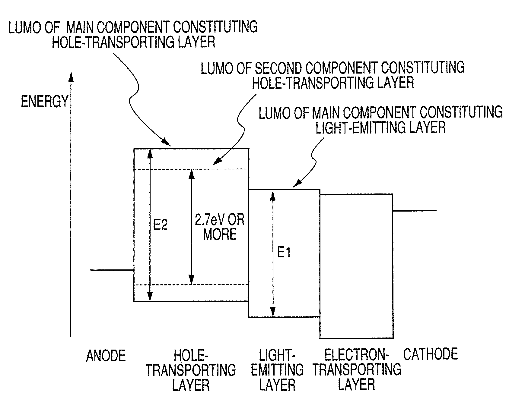
[0084]A hole-transporting layer 5 was formed by co-evaporation of TFLFL represented by the formula shown below as a main component and Compound 1 represented by the formula shown below as a second component from separate boats. The layer had a concentration of Compound 1 of 3 wt. % and a thickness of 40 nm.

[0085]

[0086]Next, a light-emitting layer 3 was formed by co-evaporation of Compound 2 represented by the formula shown below as a main component and Compound 3 repre...

example 2

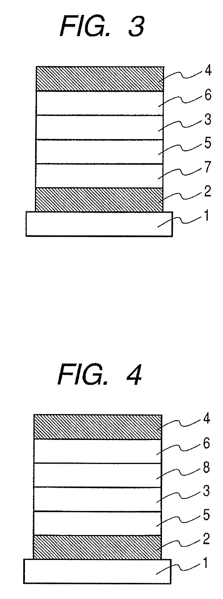
[0110]A light-emitting device was produced by following the same procedure as in Example 1 with the exception that Compound 4 shown below was used as the main component of the light-emitting layer 3; Compound 5 shown below was used as a light-emitting dopant; and αNPD and Compound 6 shown below were used as the main component and second component of the hole-transporting layer 5, respectively.

[0111]

[0112]When a voltage of 4.5 V was applied to the thus obtained device with the ITO electrode (anode) being used as a positive electrode and the aluminum electrode (cathode) being used as a negative electrode, emission of a blue light derived from Compound 5 and having a maximum emission wavelength of 450 nm with an emission luminance of 300 cd / m2 and an emission efficiency of 2.31 lm / W.

[0113]Furthermore, when a voltage was applied to the device in a nitrogen atmosphere for 100 hours so that the current density was kept at 30 mA / cm2, the device emitted light at a luminance of about 1,100 c...


PUM


Abstract

In an organic light-emitting device which uses, in particular, a light-emitting layer material having a wide band gap, a lowering in emission intensity due to continuous driving is alleviated while maintaining a high emission efficiency. There is provided an organic light-emitting device in which a hole-transporting layer contains a second component in addition to a main component; an energy of a lowest triplet excited state of the second component is less than an energy of a lowest triplet excited state of the main component of the hole-transporting layer; a lowest unoccupied molecular orbital energy of the second component is higher than a lowest unoccupied molecular orbital energy of the main component of a light-emitting layer; and the second component has an energy gap of 2.7 eV or more.

Description

BACKGROUND OF THE INVENTION[0001]1. Field of the Invention[0002]The present invention relates to a light-emitting device using an organic compound, and more specifically, to an organic light-emitting device that emits light by applying an electric field to a thin film composed of an organic compound.[0003]2. Description of the Related Art[0004]An organic light-emitting device suggests its potential to find use in a wide variety of applications owing to its characteristics such that the device can be formed into a thin, light-weight light-emitting device which shows high luminance at a low applied voltage; has a variety of emission wavelengths; and provides high-speed response. However, particularly when considering its application to, for example, a full-color display, the stability of the existing device is not sufficient for putting into practical use, so that an additional improvement in stability has been needed.[0005]Japanese Patent Application Laid-Open No. 2002-359080 disclos...

Claims


Application Information

Patent Timeline
Patent Type & Authority Patents(United States)
IPC IPC(8): H01J1/62
CPCH01L51/5012H01L51/0058H01L51/006H01L51/5048H10K85/626H10K85/633H10K50/11H10K50/14
Inventor OKINAKA, KEIJIYAMADA, NAOKISAITOH, AKIHITO
Owner CANON KK
Why Eureka
Try Eureka